


No one was surprised when Nvidia presented its GeForce GTX 1080 Ti at this year's Games Developer Conference (GDC). Surprisingly, there was only one thing: the price point of 700 dollars.
Based on the specifications of the card, the GeForce GTX 1080 Ti should be as fast as a Titan X (Pascal) – and maybe even a bit faster. So why is the price of the flagship so massively undercut? We don't have a really good answer to this question – just one guess: Nvidia AMD's Radeon RX Vega is probably on the horizon and is already setting the groundwork for future high-end disputes.
And why now? Because the GeForce GTX 1080 Ti is already available today, as Nvidia tells us – and because that doesn't apply to Vega, we'd add biting.
Committee shows winning qualities
There are currently two graphics cards based on Nvidia's GP102 GPU: Titan X (Pascal) and Quadro P6000. The former uses a version of this GPU that disables two of its streaming multiprocessors. The latter, on the other hand, installs an untouched GP102 without any errors.
However, we are talking here about a chip with 12 billion transistors. Surely the yield is not so good that all the GPUs produced fall into one of these two categories, right? This is where the GeForce GTX 1080 Ti comes in.
The 1080 Ti uses a similar streaming multiprocessor configuration to the Titan X: 28 of its 30 SMs are enabled, resulting in 3584 CUDA cores and 224 texture units. Nvidia raises the processor's base clock to 1480 MHz and quantifies the GPU's typical boost clock at 1582 MHz. By comparison, the Titan X (Pascal) clocks at 1417 MHz and 1531 MHz respectively.
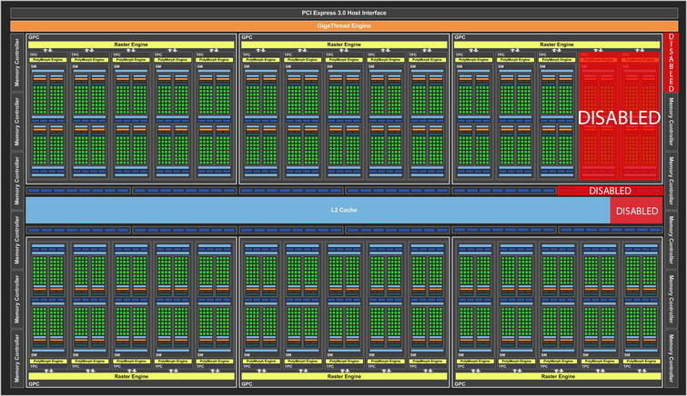
For the backend, however, the new GeForce card differs from Titan X and Quadro P6000. The latter two cards use all 12 32-bit memory controllers, ROP clusters, and L2 cache blocks of the GP102, leaving no room for error. Instead of entering marginally faulty GPUs in the ton, they are turned into GTX 1080 Ti's by disabling a storage controller, a ROP partition, and 256 kilobytes of L2 cache.
The result may need to get used to on the data sheet, but it is absolutely functional: The GTX 1080 Ti has an aggregated memory interface of 352 bits, 88 ROPs and 2816 kilobytes of L2 cache. By comparison, the Titan X has a 384-bit wide data path, 96 ROPs, and smooth three megabytes of L2 cache.
If you look at it like this, the GeForce GTX 1080 Ti should be slightly disadvantaged compared to the Titan X. But in the months since the launch of the GTX 1080, Micron has launched 11 (and 12) Gbps of fast GDDR5X storage. Its higher data rate easily compensates for the narrower memory bus: On paper, the GTX 1080 Ti with 484 GByte/s beats even the Titan X with its 480 GByte/s.
Of course, the maximum storage capacity of the card is affected by the elimination of a storage channel. But a storage capacity of 11 instead of 12 gigabytes doesn't really sound alarming when you compare it to a four-gigabyte Radeon R9 Fury X, which also performs in 4K resolutions.
A loss of storage capacity is also better than repeating the GTX-970 disaster: On the GeForce GTX 970, Nvidia removed a ROP and an L2 block, but left the memory at the old size, resulting in significantly slower access to the orphaned 512-MByte storage segment. On the other hand, the 11 gigabytes of GDDR5X memory on the GTX 1080 Ti communicate at full speed.
Specifications
| Quadro P6000 |
Titan X (Pascal) |
GeForce GTX 1080 Ti |
GeForce GTX 1080 |
GeForce GTX 980 Ti |
|
|---|---|---|---|---|---|
| Gpu |
GP102 | GP102 | GP102 |
GP104 | GM200 |
| CUDA cores |
3850 | 3584 | 3584 |
2560 | 2816 |
| Base clock | 1506 MHz | 1417 MHz | 1480 MHz |
1607 MHz | 1000 MHz |
| Boost clock |
1645 MHz | 1531 MHz | 1582 MHz |
1733 MHz | 1076 MHz |
| Memory Size & Type |
24 GByte GDDR5 | 12 GByte GDDR5X | 11 GByte GDDR5X |
8 GByte GDDR5X | 6 GByte GDDR5 |
| The size |
471 mm2 | 471 mm2 | 471 mm2 |
314 mm2 | 601 mm2 |
| Technology |
16 nm | 16 nm | 16 nm |
16 nm | 28 nm |
| Transistors |
12 billion | 12 billion | 12 billion |
7.2 billion | 8 billion |
| Streaming Multiprocessors (SM) |
30 | 28 | 28 |
20 | 22 |
| GFLOPS (basic clock) |
10.883 | 10.157 | 10.609 |
8.228 | 5.632 |
| Texture Units |
240 | 224 | 224 |
160 | 176 |
| Texture fill rate |
361.4 GT/s | 317.4 GT/s | 331.5GT/s | 257.1 GT/s | 214 GT/s |
| Rops |
96 | 96 | 88 | 64 | 96 |
| Pixel fill rate |
144.6 GPix/s | 136 GPix/s | 130.24 GPix/s | 114.2 GPix/s | 116.7 GPix/s |
| Storage data rate |
9 GByte/s | 10 GByte/s | 11 GByte/s | 10 GByte/s | 7 GByte/s |
| Storage bus |
384 bits | 384 bits | 352 bits |
256 bits | 384 bits |
| Memory bandwidth |
432 GByte/s | 480 GByte/s | 484 GByte/s |
320 GByte/s | 336 GByte/s |
| L2 cache |
3 MByte | 3 MByte | 2816 KByte |
2 MByte | 3 MByte |
| Tdp |
250 watts | 250 watts | 250 watts |
180 watts | 250 watts |
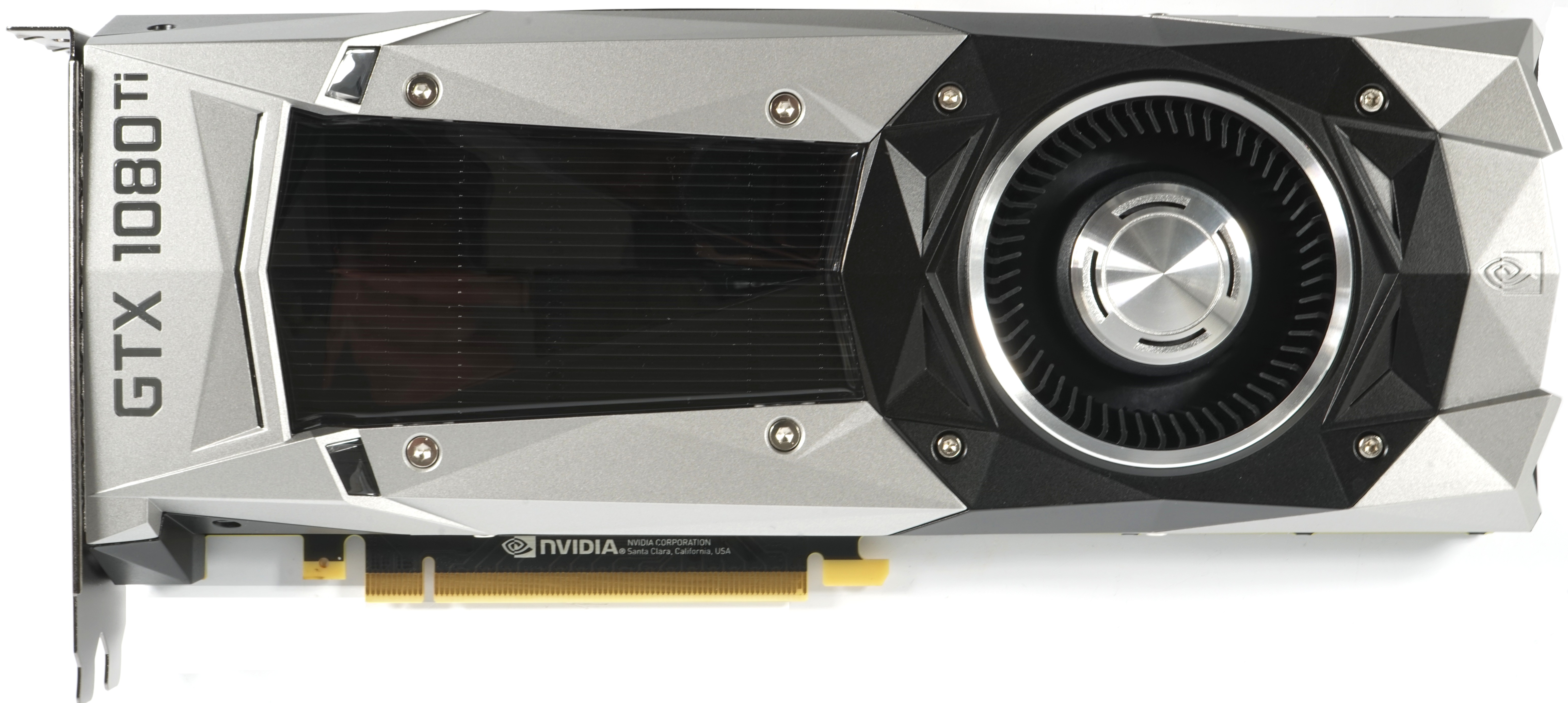
Say "Hello!" to the GeForce GTX 1080 Ti Founders Edition
Nvidia said when introducing the map that the cooler has changed significantly compared to the Titan X (Pascal), which is not noticeable at this time. But in the course of ours we will come back to this again. With the exception of the label, everything has actually been completely taken over. This also applies to the material mix of cast aluminium and plastics, as well as the optically dominant radial cooler with a net diameter of 6.2 cm.
 |
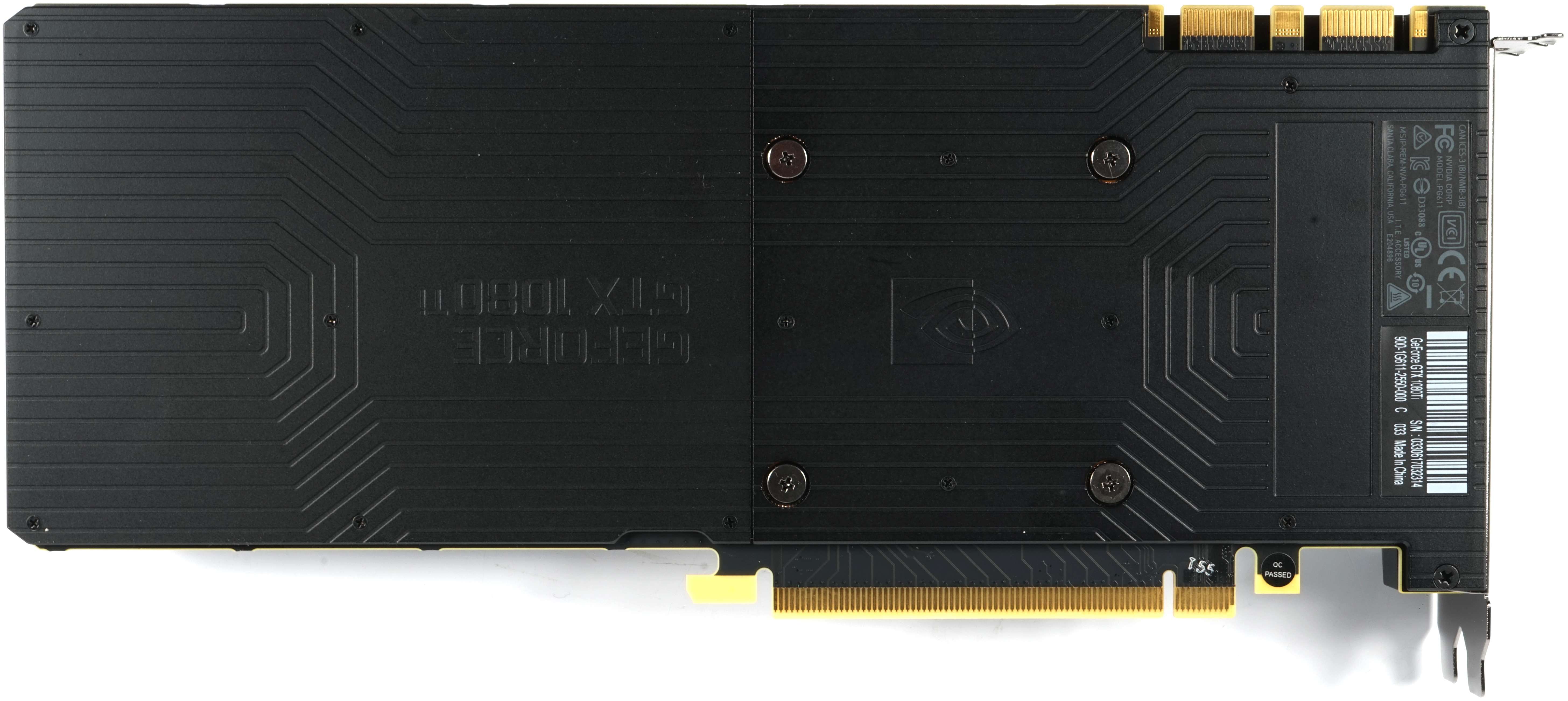 |
Mt 26.9 cm from the exterior of the slot aperture to the radiator end, the dimensions compared to the Titan X (Pascal) have not changed, which also applies to the installation height of 10.5 cm from the top edge of the motherboard slot to the radiator top edge. The installation depth of 3.5 cm also stands for the already known dual slot design, while the weight of the card has increased a little to 1039 grams.
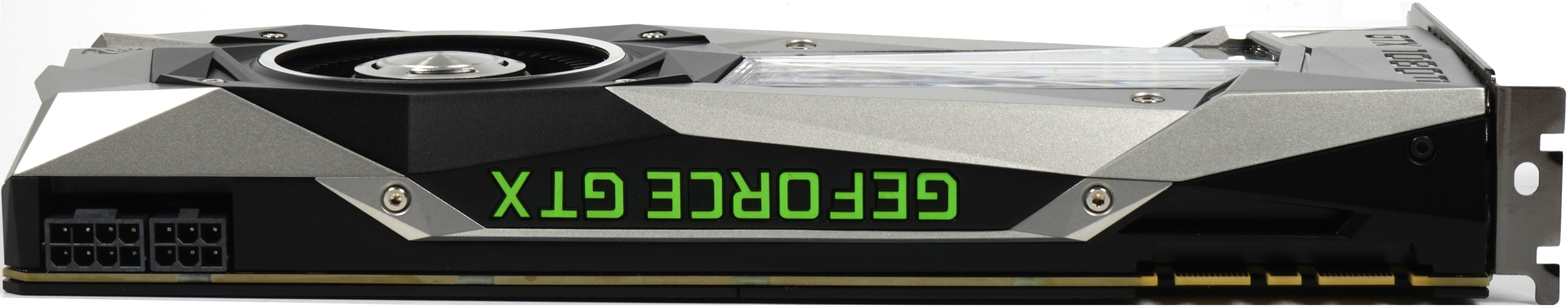
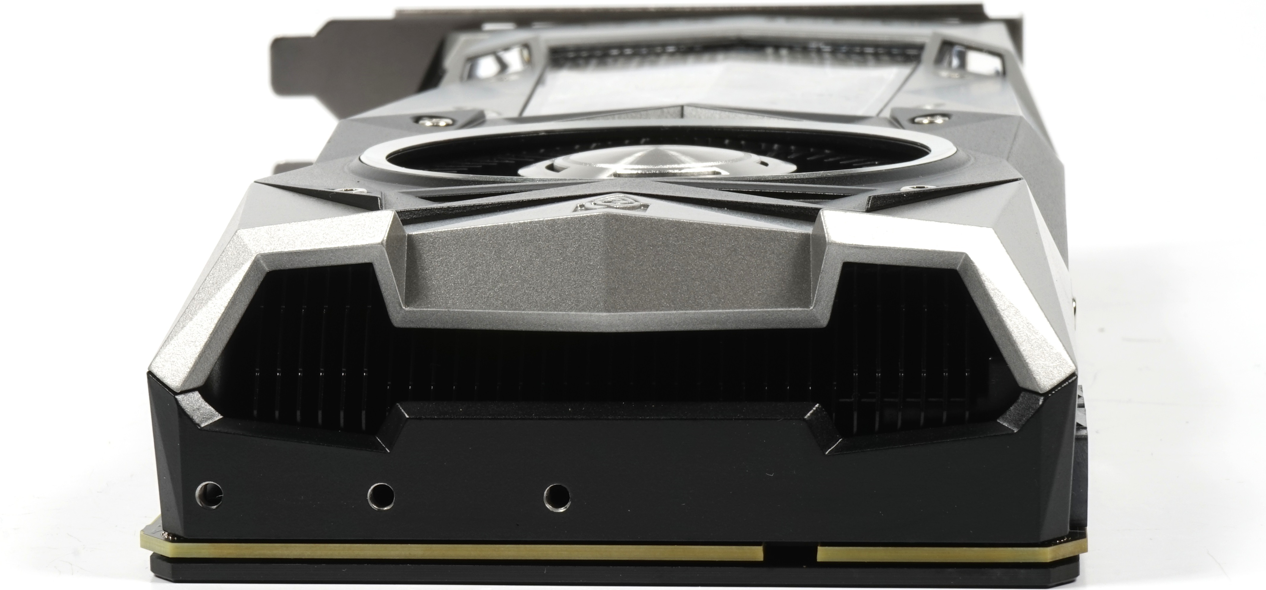
The top also gives itself in the usual picture and shows next to the green illuminated lettering an 8- and 6-pin external power supply connection. The underside is even more unspectacular and shows besides the cover actually … Nothing.
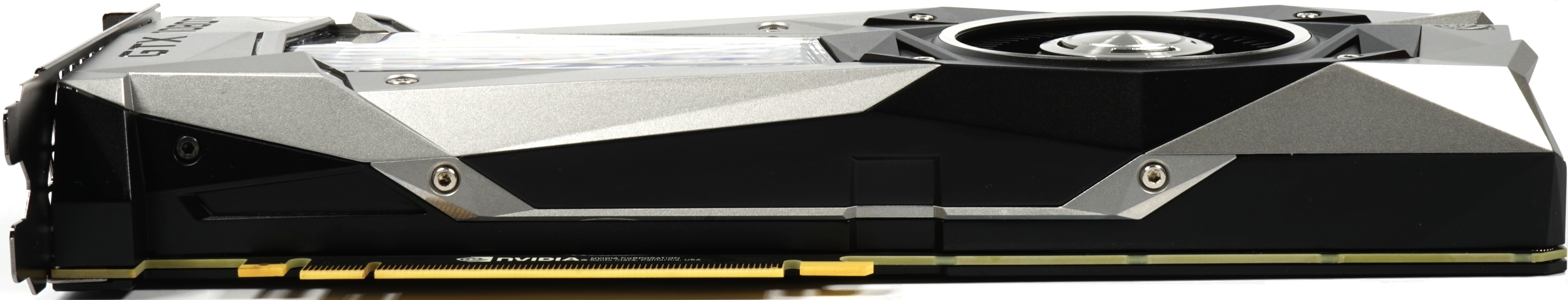
The end of the card provides the usual air openings for a part of the air outlet, whereby it can be assumed from the plate design that the heat dissipation into the interior of the housing is rather marginal. But with regard to the concrete values, we will look at the measurements in a while.
 |
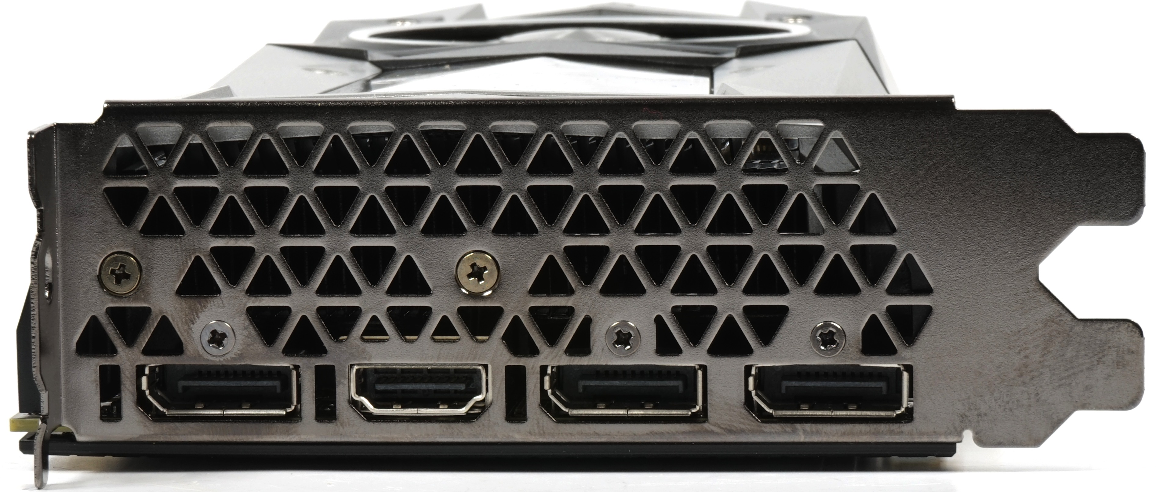 |
To improve the air outlet at the slot aperture, Nvidia has completely dispensed with the DVI connector and offers instead only three DisplayPort ports and one HDMI. The rest is dominated by the ventilation grille.
Radiator construction
Nvidia mainly uses very thin sblocks (0.5 mm) to attach the two-piece backplate, whose counter-thread in turn sits in the screw head of Nvidia's special piggyback screws below the backplate. These rather unusual hexagonal screws (M2.5) are used at the same time to attach the complete housing to the board.
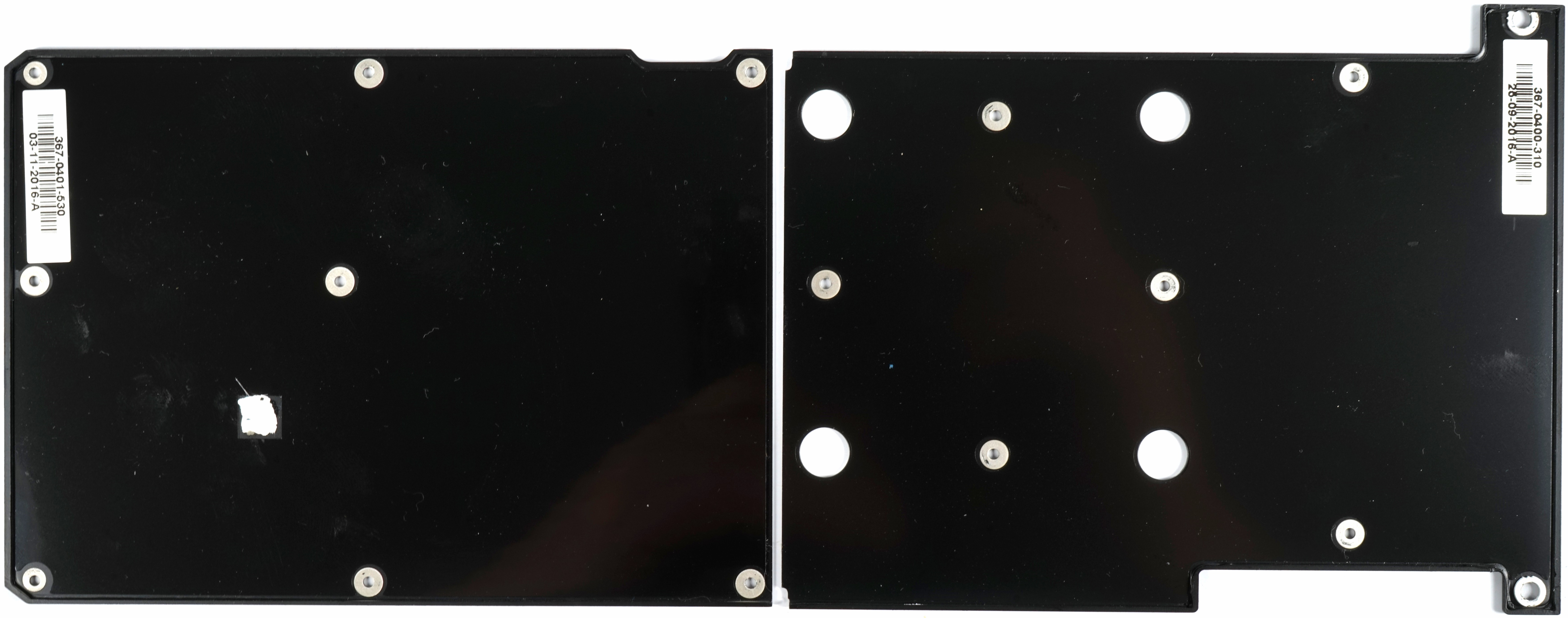
The first change has already become apparent, because Nvidia connects the PWM controller chip on the back of the board with a thick thermal conductive fleece, which is actually rarely used, with the one backplate half for better heat dissipation. This would work even better if Nvidia had simply omitted the plastic film with which the backplate is glued inside.
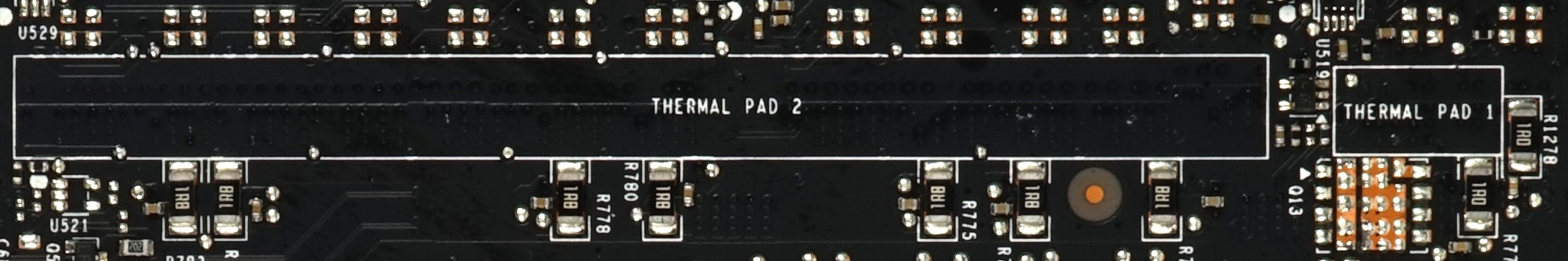
If we take a quick look at the exposed back of the board, then we see half left two marked areas labeled with "Thermal Pad 1" and "Thermal Pad 2", but in the final product the provided pads are missing. Whether Nvidia has simply left the courage (or even the lust) here, we cannot judge – and must not measure anything yet.
In addition to the usual thermal pads for voltage converters and memory, the solid plate of the radiator frame again carries some of the aforementioned nonwoven strips, which additionally connect active components such as VR chips, MOSFETs and diodes thermally to the bottom of the large plate. . We have not been able to make any other changes to the cooler so far.
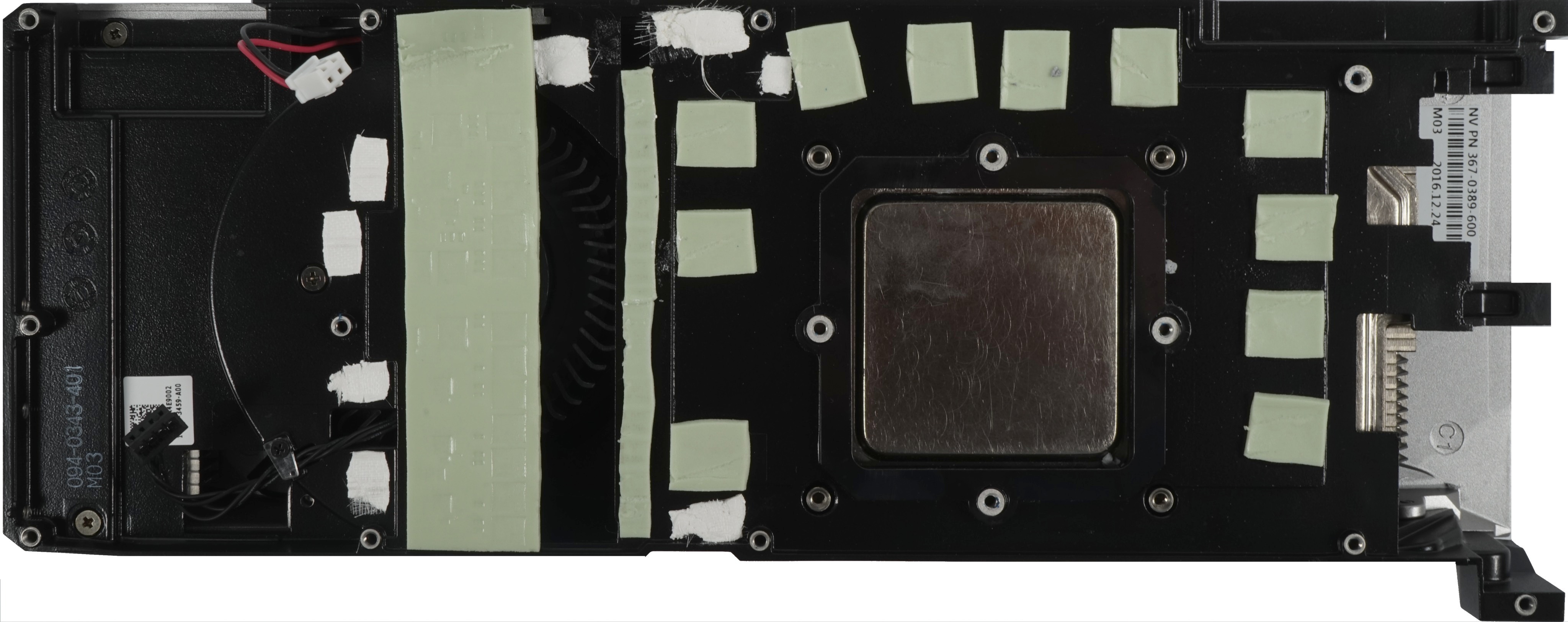
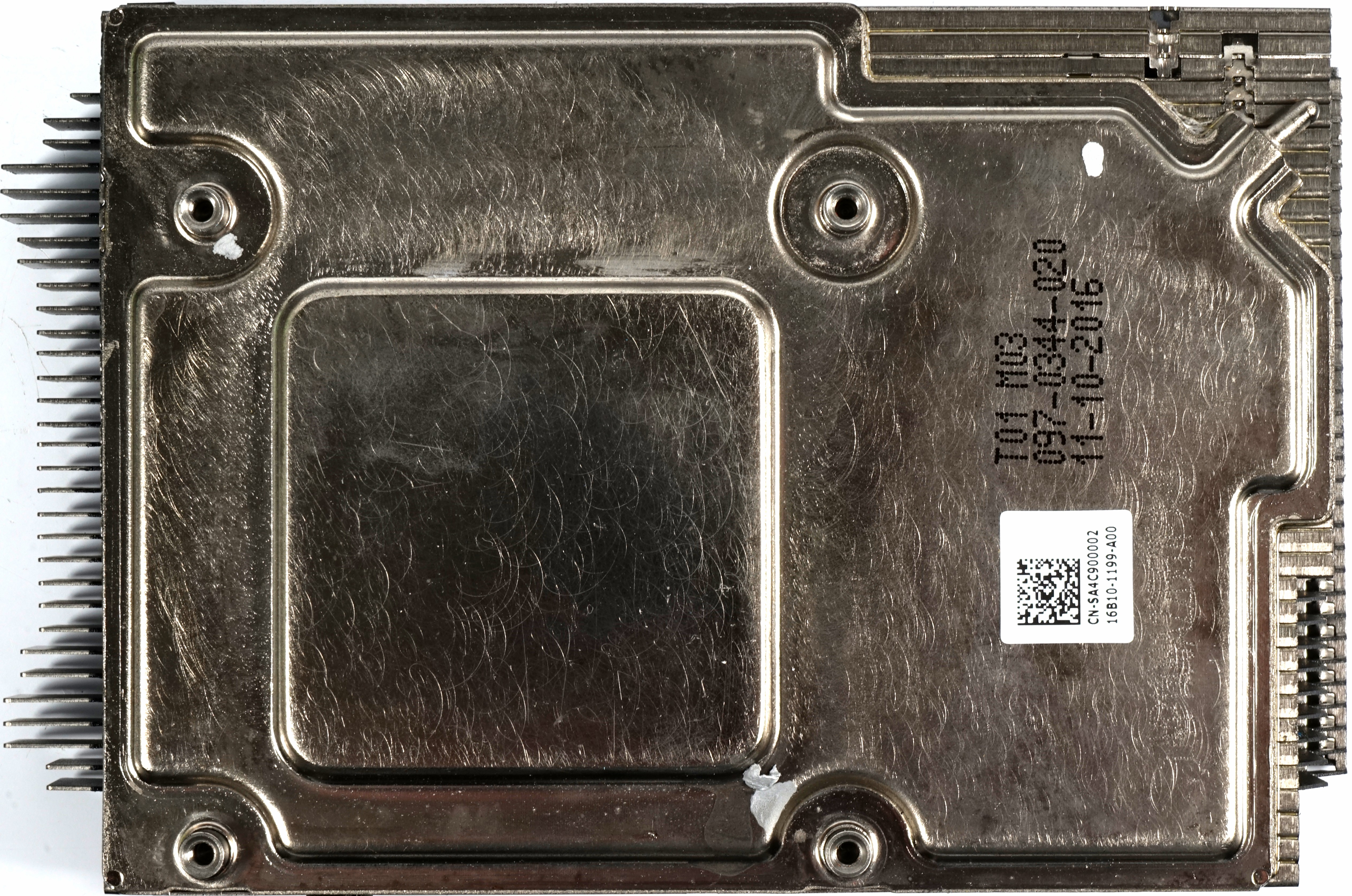
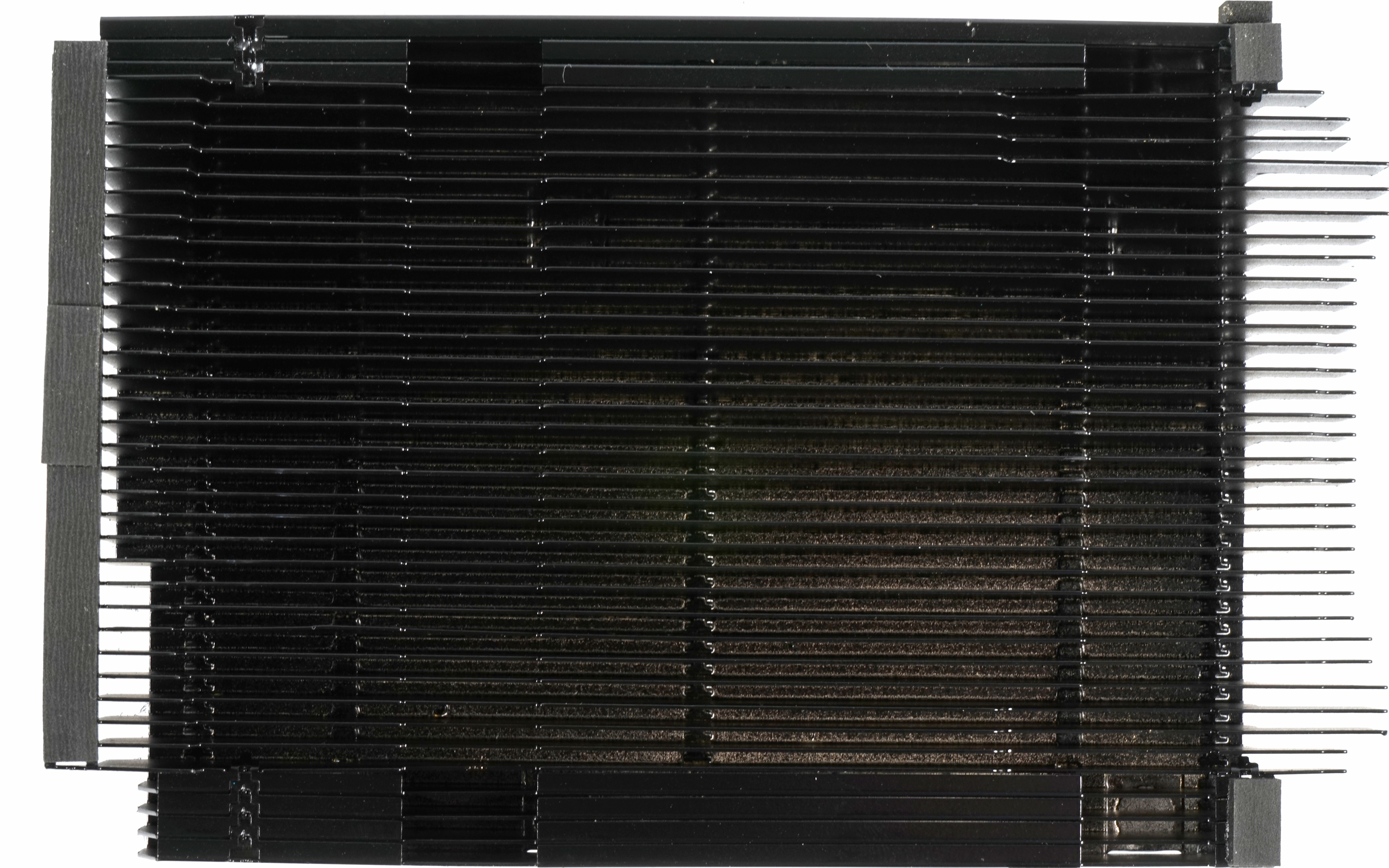
As with the other Founders Edition (FE) cards, Nvidia again relies on a vapor chamber inserted into the ground, which is attached to the board with four spring screws and represents the actual GPU cooler. The rest is cooled over the large frame as already described.
 |
 |
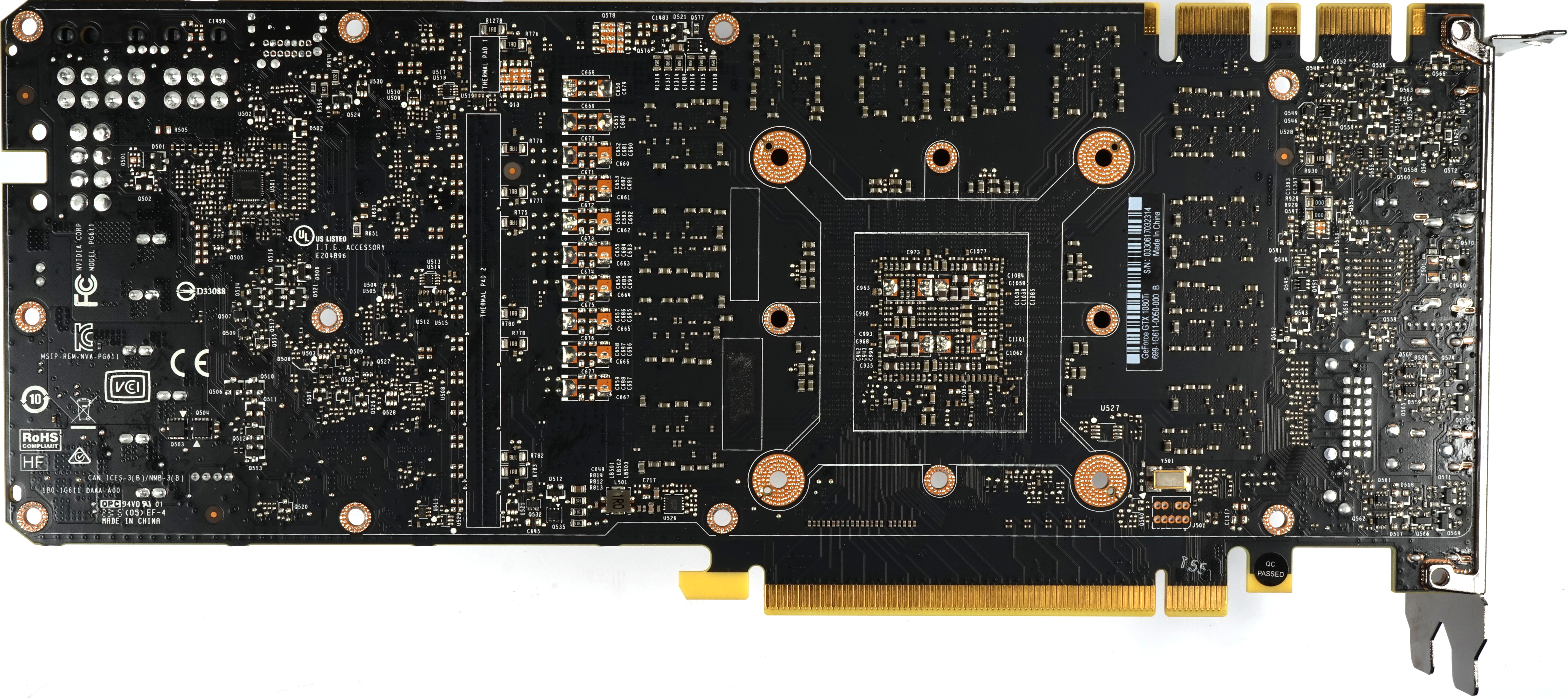
Board design and components
Finally, let's take a look at the board and the improvements announced by Nvidia. What is striking at first glance: The range of voltage converters has now undergone a full assembly compared to the Titan X (Pascal), even if it is still the same board.
Nvidia has been using this common base since the Quadro P6000, whose 8-pin supply connection is on the rear, which can be clearly seen on the eight unoccupied soldering eyes.
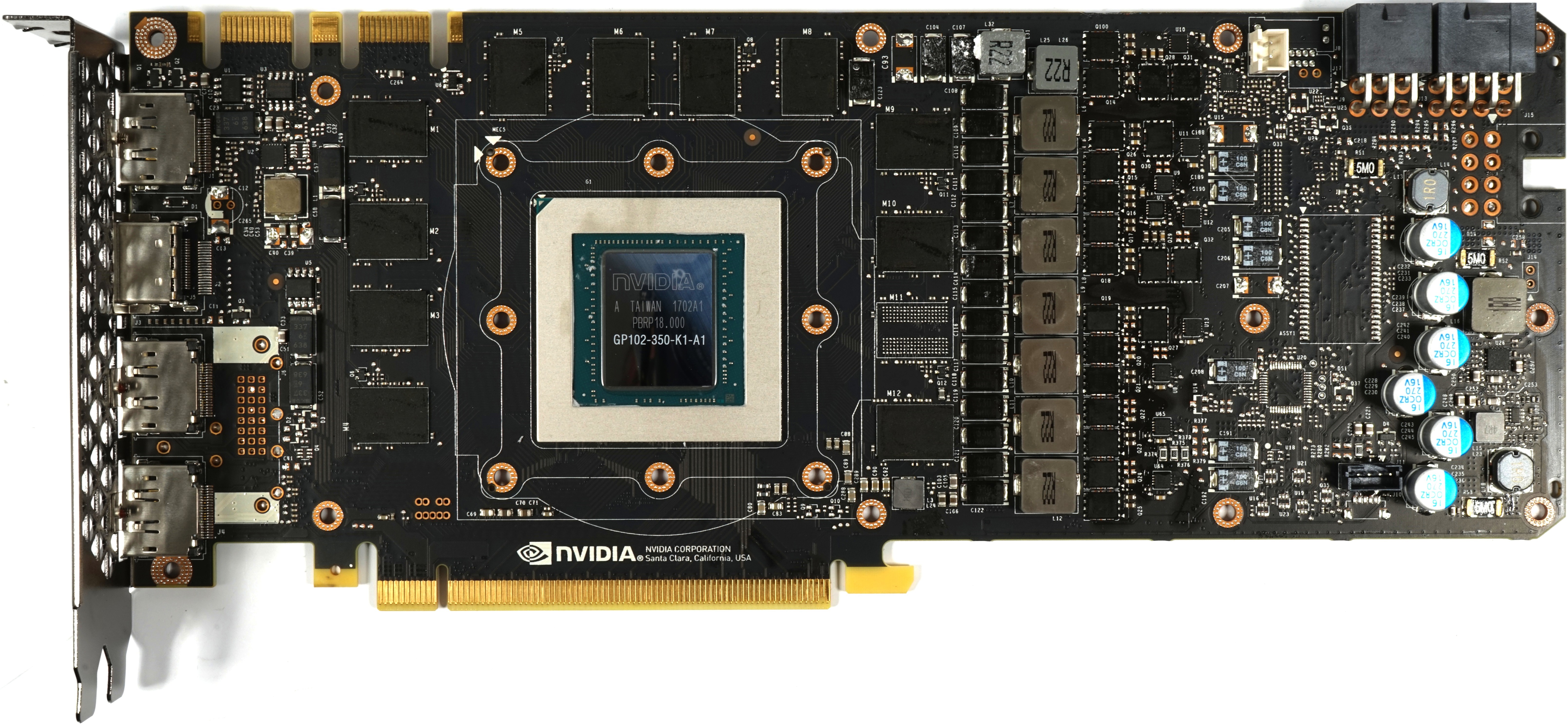
But let's take a quick look at the memory, where, unlike the Titan X (Pascal), a module is missing.
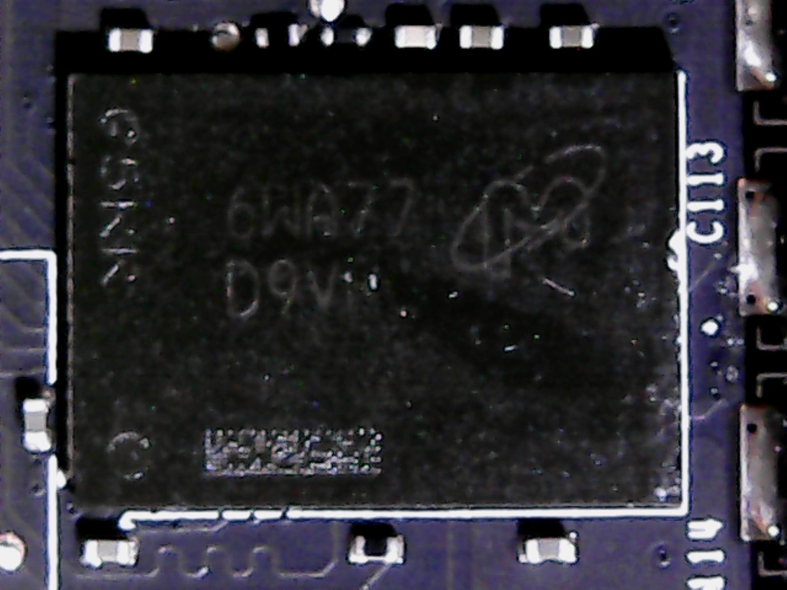 A total of 11 of the new G5X-Micron modules of type MT58K256M321-Ja110, which offer up to 11 GByte/s and are therefore intended to compensate the missing 32 bits of the memory interface with a higher clock speed of 5500 MHz (effectively), are installed on this card.
We are somewhat surprised that Nvidia didn't install the MT58K256M321-Ja120, which clocks a little higher. But one is probably afraid of a thermal problem of the storage tank operated with up to 1.35 volts, which in both cases may get hot up to a maximum of 95°C.
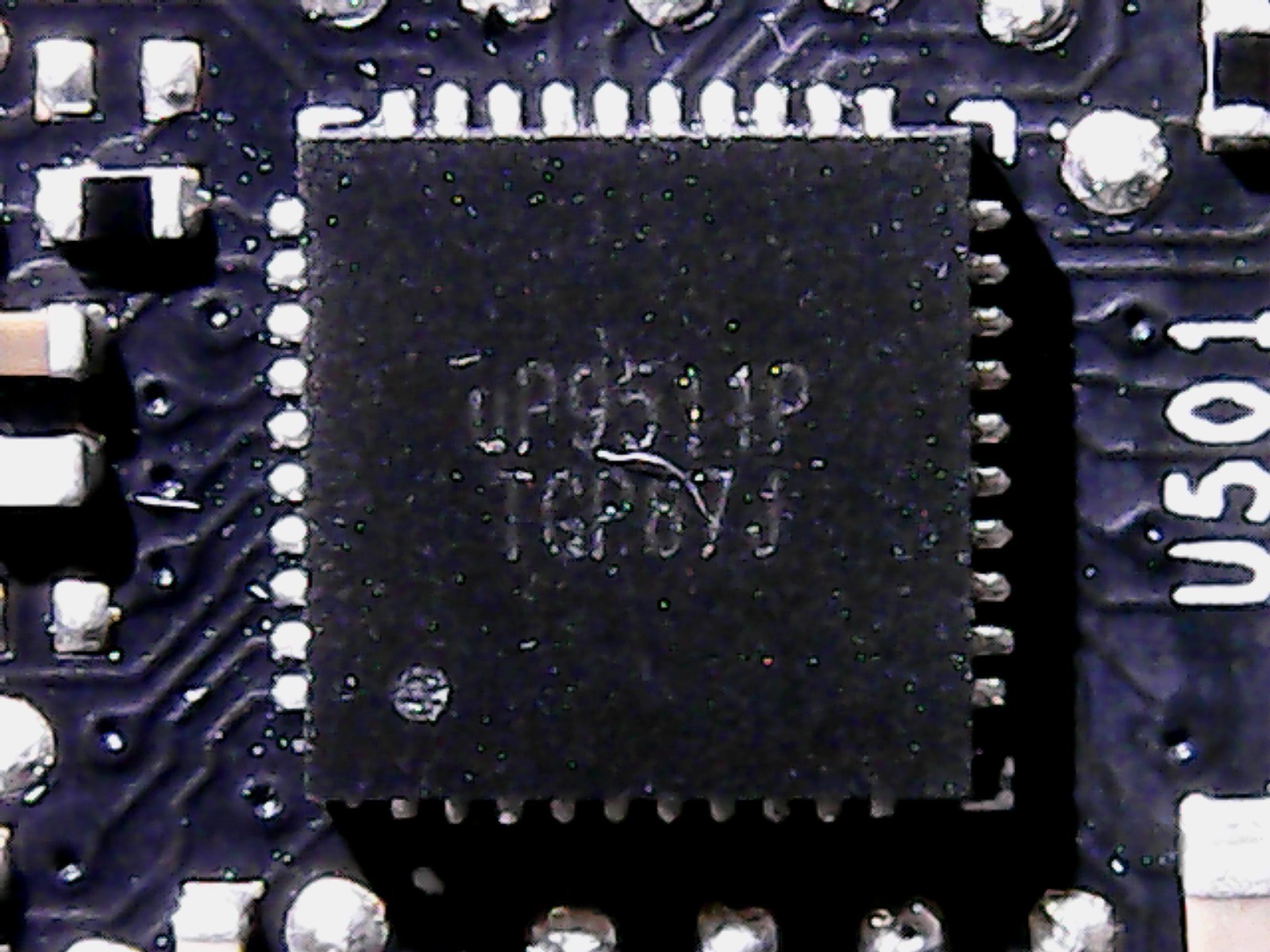
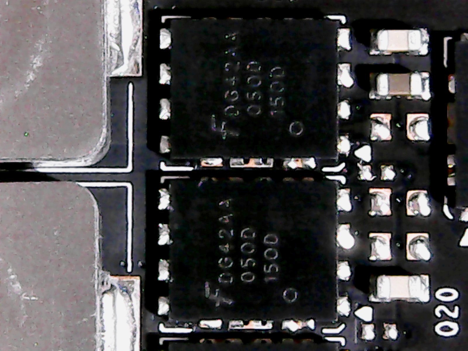
With the voltage converters, Nvidia stays true to itself and relies on a good old acquaintance with the uP9511 for the GPU and its seven phases, which can be found as usual on the back of the board.
This component selection for the PWM controller makes perfect sense, as it can operate the seven phases simultaneously and not only control 6(+2) phase designs.
 |
 |
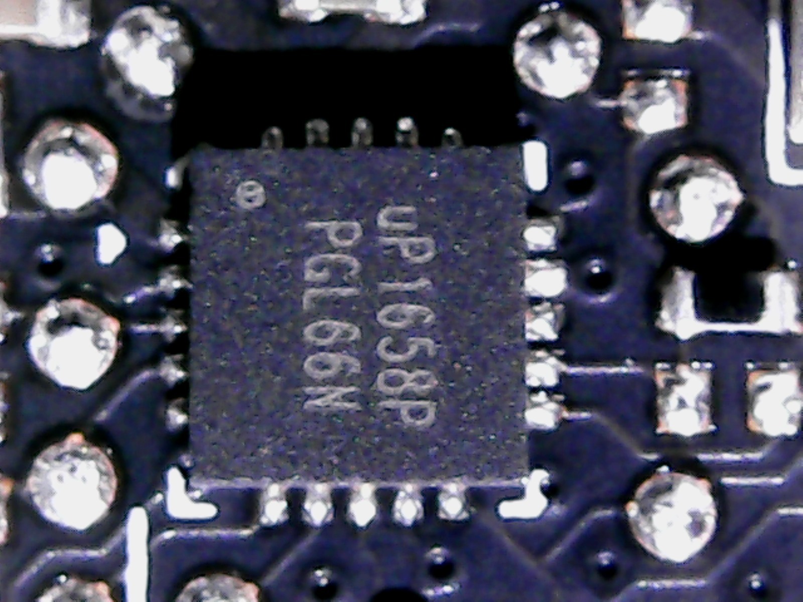
The design of the voltage converters is interesting in that Nvidia relies on a rather simple design made of simple buck converter (LM53603) for the high-side and now two instead of a MOSFET on the low-side, which in the form of two Fairchild-D424-N-Channel MOSFETs. This slightly equalizes the hotspots, because the power dissipation is thus distributed over a twice as large area.
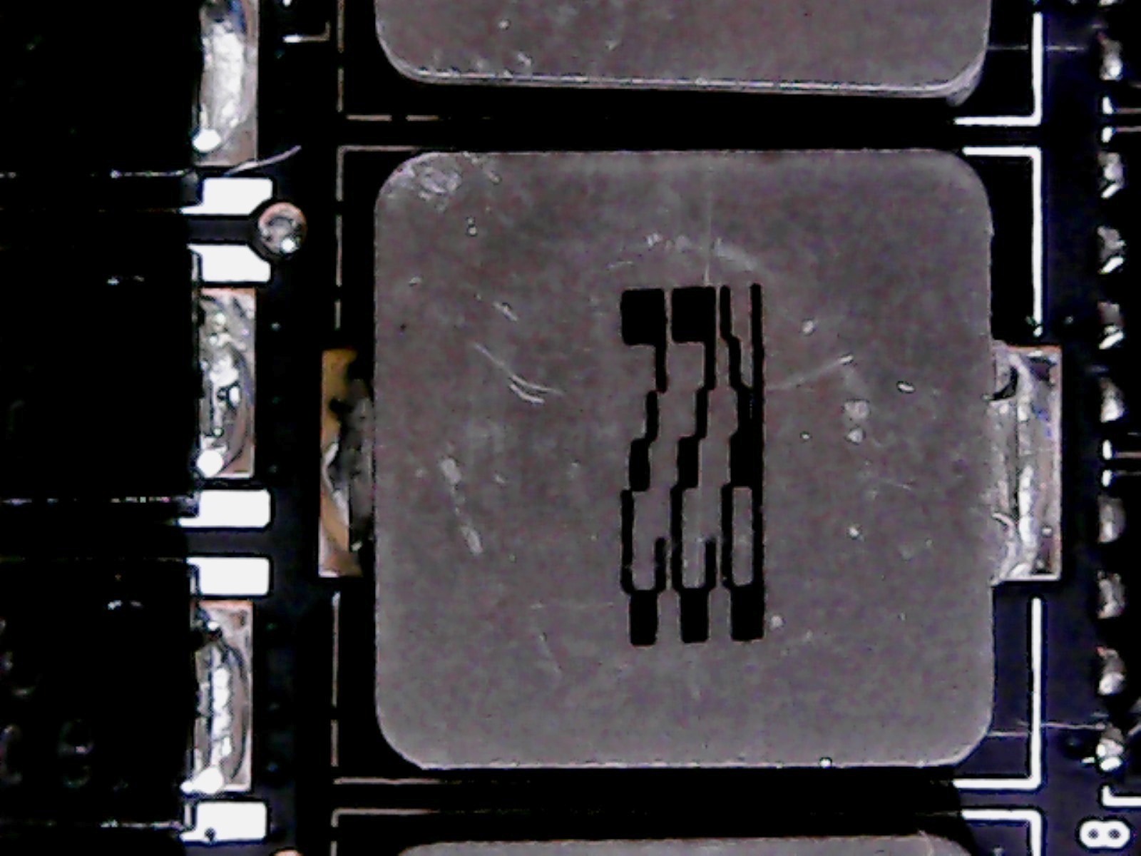
The coils rely on simply encapsulated ferrite trays, which are qualitatively equivalent to Foxconn's Magic coils, can be machine-mounted and are not plugged through. Thermally, this is an advantage for the back of the board, whereby Nvidia incomprehensibly does not cool the hot coils, but only the adjacent capacitors.
 |
 |
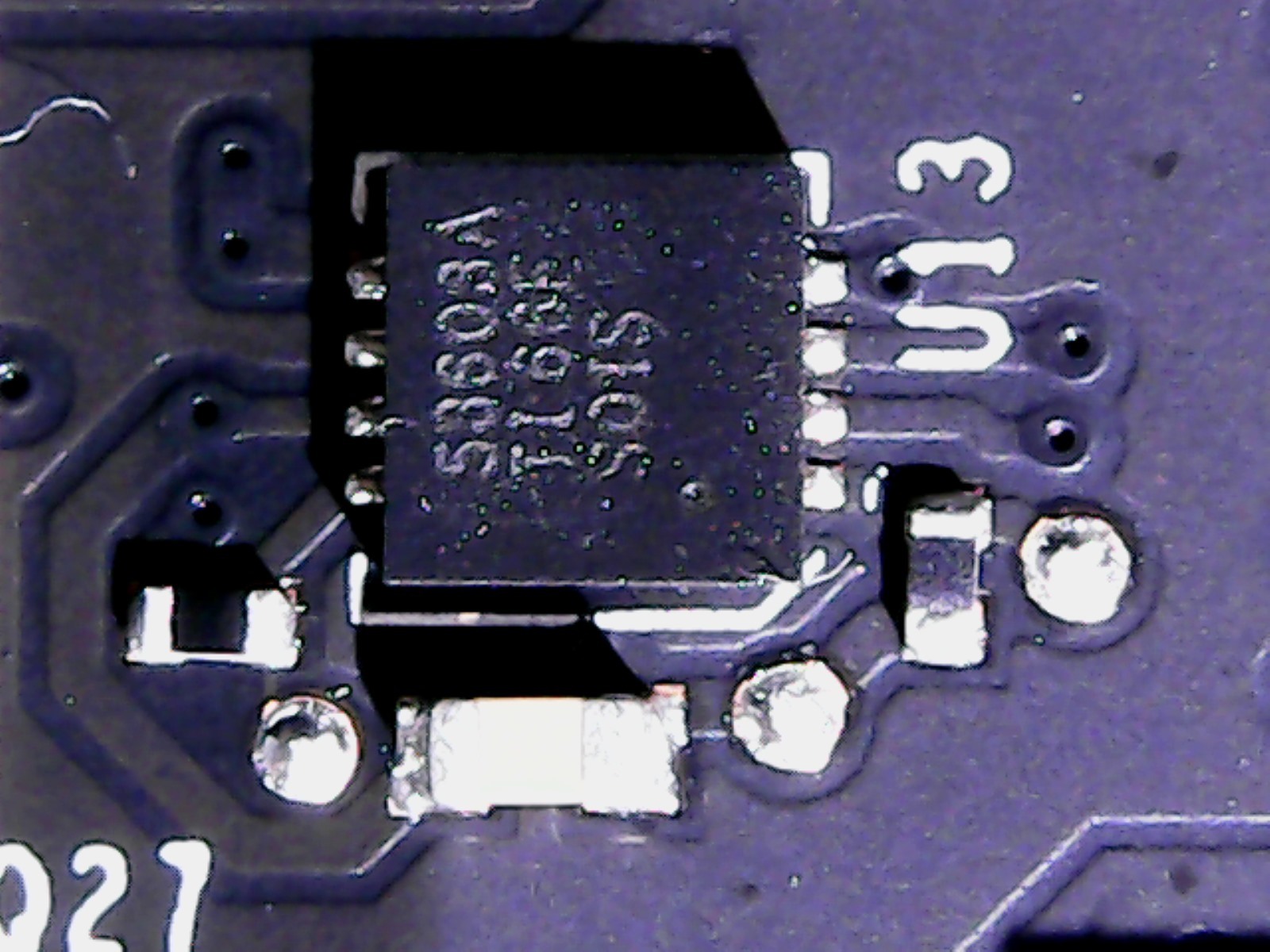
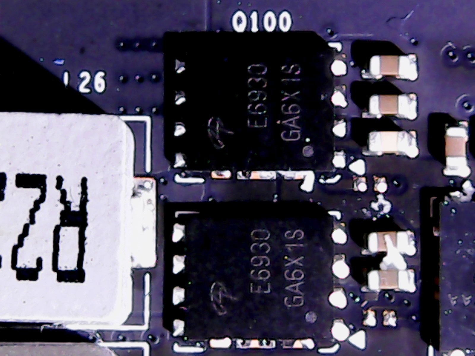
The memory is fed via two parallel controlled phases, which are controlled by an uP1685. The low-side is solved via two dual-N-channel logic-level PowerTrench-MOSFETs E6930, which is rather unusual, the high-side with the already mentioned FD424. The coils are then correspondingly smaller for these two simpler phases.
 |
 |
So what about the new cooler design mentioned? Now that we know the correct readings, we would better describe and rewrite it as a new cooling concept, where both the active components and the waste heat dissipation with additional pads are among the most obvious changes. In any case, we have not been able to see any more things that could bring significant improvements.
MORE: Nvidia GeForce GTX 1080 and GTX 1070 Roundu
p
MORE: Nvidia GeForce GTX 1060 Roundu
p
How we test the GeForce GTX 1080 Ti
Nvidia's new addition will no doubt find a new home in high-end platforms; everything else simply makes no sense. Some of these systems will be based on Intel's Broadwell E CPUs, but we are loyal to our Core i7-7700K, which is based on an MSI Z170 Gaming M7. In addition, there is the G.Skill storage kit F4-3000C15Q-16GRR.
Intel's Skylake architecture is still the manufacturer's most efficient per-clock – and the base clock of 4.2 GHz is higher than the more cores of the models. The rest of the test system consists of Crucials MX200-SSD, Noctua's NH-12S CPU cooler, the 850-watt be quiet power supply! Dark Power Pro 10.
In terms of competition, the GeForce GTX 1080 Ti currently has only the GeForce GTX Titan X (Pascal), which is almost twice as expensive at 1200 dollars. The only two other competing products that make sense are Nvidia's GeForce GTX 1080 and 1070, as well as AMD's flagship Radeon R9 Fury X. We are adding a GeForce GTX 980 Ti to show how far the GTX 1080 Ti has left its predecessor behind.
Drivers and benchmarks
On the software side, there are more important changes. Our benchmark selection now includes Ashes of the Singularity, Battlefield 1, Civilization VI, Doom, Grand Theft Auto V, Hitman, Metro: Last Light, Rise of the Tomb Raider, Tom Clancy's The Division, Tom Clancy's Ghost Recon Wildlands and The Witcher 3. So we said goodbye to Battlefield 4 and Project CARS, but added several new games.
In the article THDE, we have internally described our test procedure including the underlying methodology: How we measure and evaluate the graphics performance. To sum it up, all games are rated with a combination of OCAT and our own GUI for PresentMon; the data is logged by aidA64. If you want to know more about our chart methodology, read the linked article warmly.
All values in today's test have been recalculated with updated drivers. For the Nvidia cards we use the build 378.78 and for AMD's graphics cards we use the Crimson ReLive Edition 17.2.1 – the most recent driver at the time of testing.


Kommentieren