


Teardown
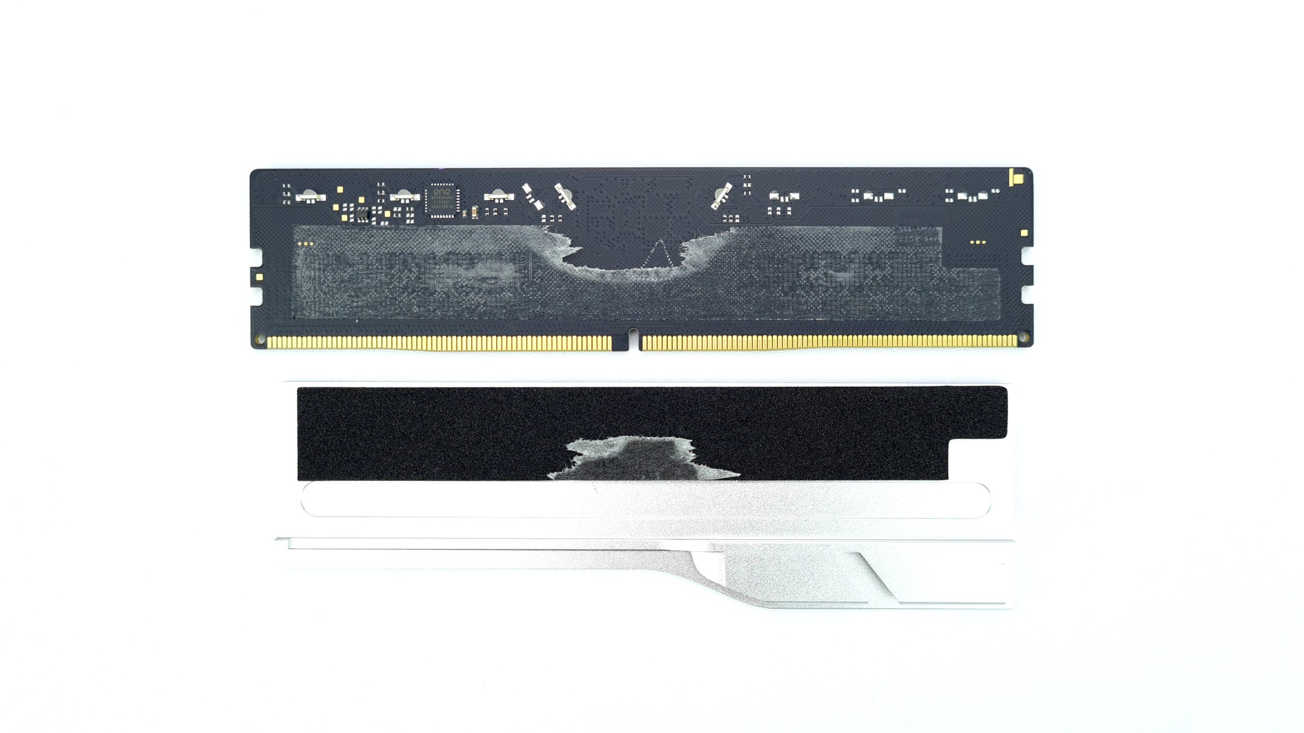
To disassemble the modules, they should be heated beforehand to loosen the adhesive. The aluminum halves can then simply be carefully levered off. In addition to the removed radiator half, the white acrylic lightspreader is now also immediately loosened. The cooler halves are actually only attached to the RAM components with a double-sided adhesive thermal pad. Unfortunately, the two outer modules are not completely covered here, which could potentially lead to a thermal bottleneck. Furthermore, the PMIC is unfortunately not connected to a pad to the cooler with a surrounding component and therefore has to dissipate its waste heat in another way.
On both sides, there are 5 RGB LEDs on the top edge each, which shine into the acrylic part from below and provide even illumination. The RGB controller with its DC-DC converter is then also located on the back. Incidentally, the adhesive here is also easy to remove after heating without the foam pad running the risk of tearing. Thus, G.Skill has found a perfect compromise when it comes to mounting, since the coolers otherwise sit bombproof and do not give the impression that they could fall off at any time.
PCB analysis
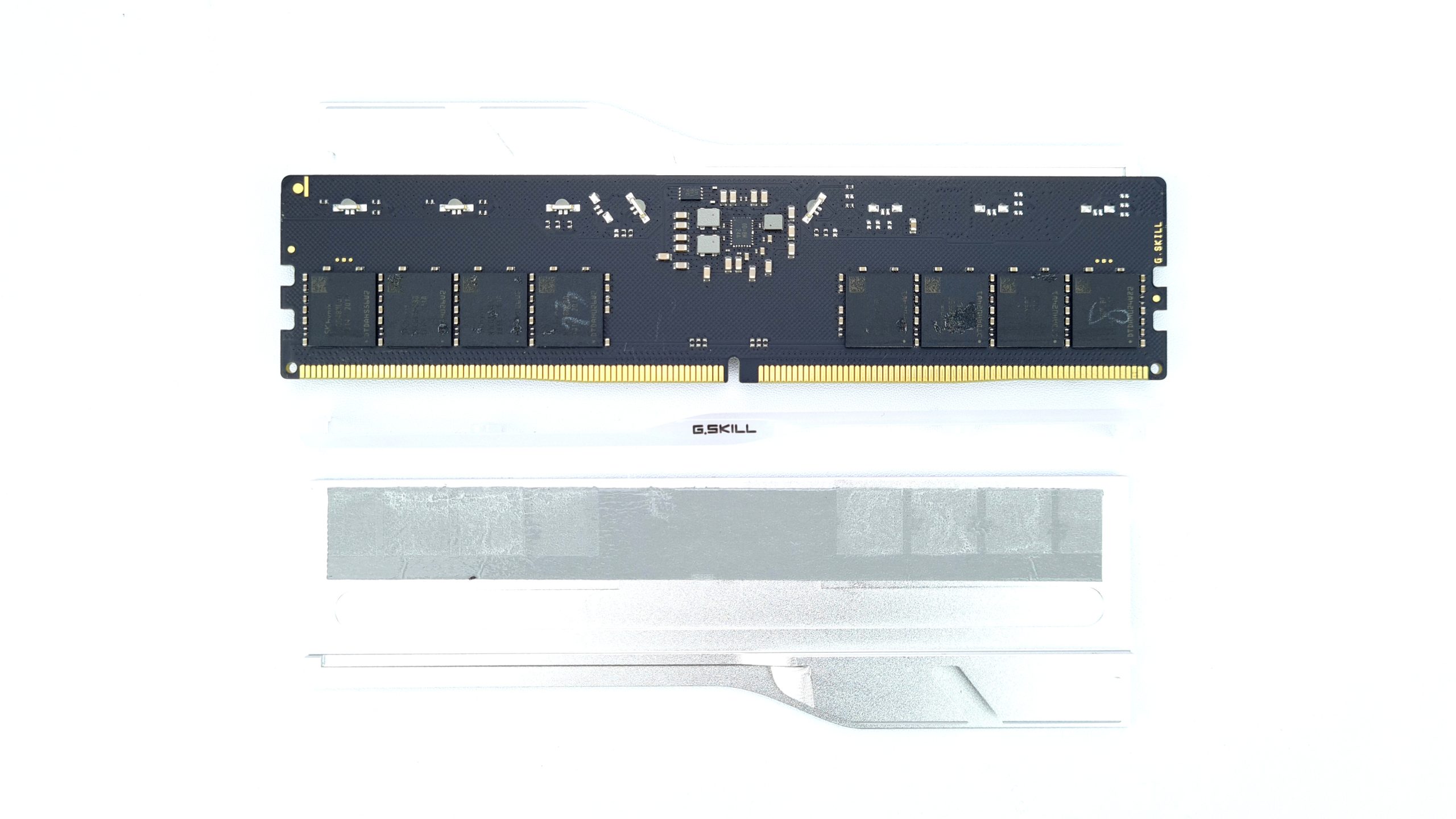
The board itself is with its dimensions identical to the A0 JEDEC reference and therefore also well suited for other coolers or water blocks. The grounding layer on the top is striking, which should provide better shielding and thus signal integrity. Unfortunately, there is no indicator for the layer count, only a golden G.Skill lettering adorns the edge of the PCB.
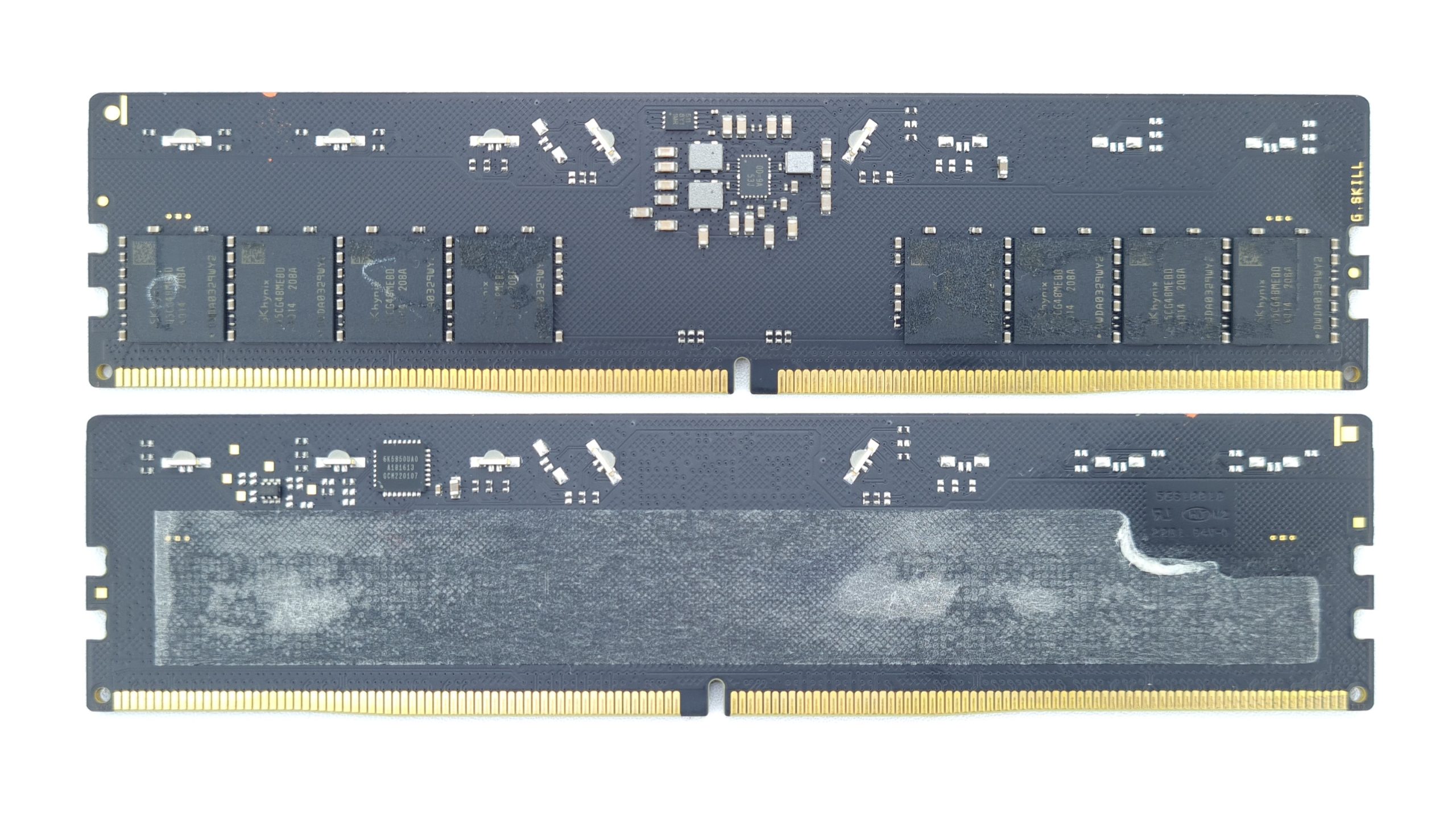
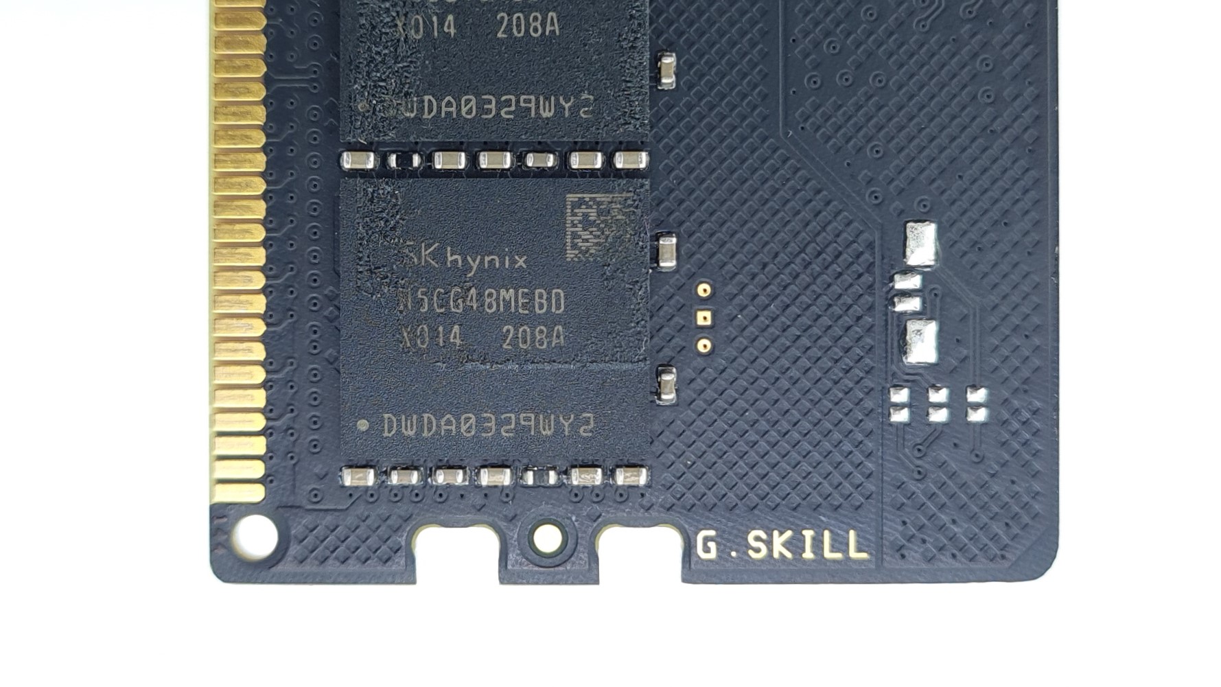
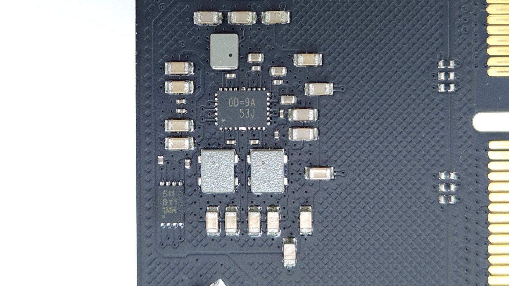
Of course, 16 Gbit M-Die ICs from SK Hynix with the part number H5CG48MEBD are used as memory components. The PMIC is a component with the rather inconspicuous label 0D-9A 53J, although we can already identify it as being manufactured by Richtek from previous tests. The SPD EEPROM is labeled “511 8Y1 1HL”, whereby it is a Renesas make.
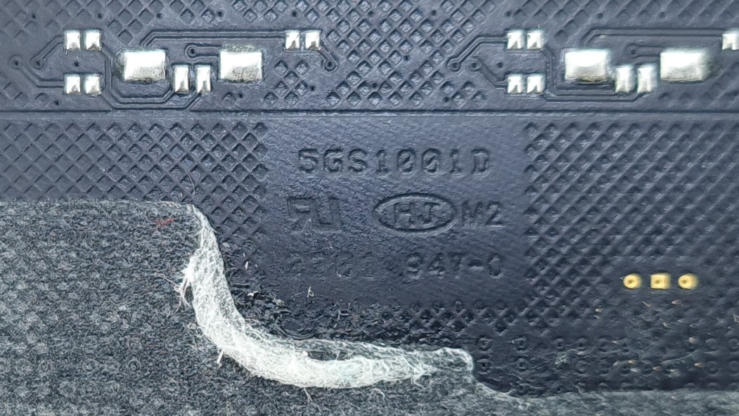
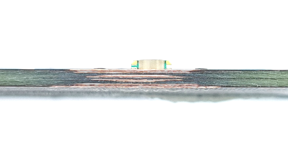
On the back, the PCB bears an embossing that tells us the manufacturer. The logo shows Hsien Jinn from Taiwan. Usually the boards of this manufacturer carry a “KO number” – the website domain is even kopcb.com. Instead, the string 5GS1001D is found here, where the first 3 characters should stand for DDR5 G.Skill and the 10 could indicate the layer count. Because if we take the good old sandpaper to hand, a 10-layer design actually reveals itself, which in turn could explain the board’s special nomenclature.
For comparison, the Teamgroup DELTA 6400c40 modules from the past test use an 8-layer design from the same manufacturer with a “KO number”. Finally, there is a reference to the week of manufacture here with 2201 – 1. Calendar week of 2022 – and the usual safety certification notices – the “RU” logo and Underwriters Laboratories (UL) 94V-0 marking for the North American market.


14 Antworten
Kommentar
Lade neue Kommentare
Urgestein
Veteran
Mitglied
Urgestein
Veteran
Urgestein
Urgestein
Urgestein
Urgestein
Urgestein
Urgestein
Veteran
Neuling
Neuling
Alle Kommentare lesen unter igor´sLAB Community →