


SPD Information
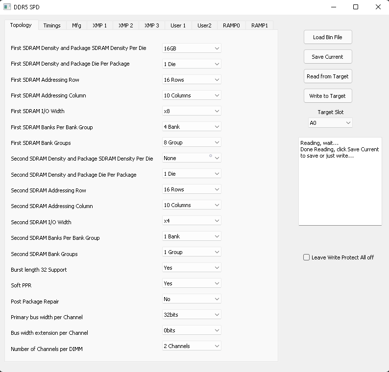
As always with RAM modules, a look at the built-in “identity card”, the SPD, is not to be missed. The Asus “Worktool” software with the “DDR5 SPD” function is used here again to read out and visualize the information. We don’t find anything unexpected in the Topology tab. These are single-ranked modules with 8 ICs of 16 Gbit capacity with an x8 interface.
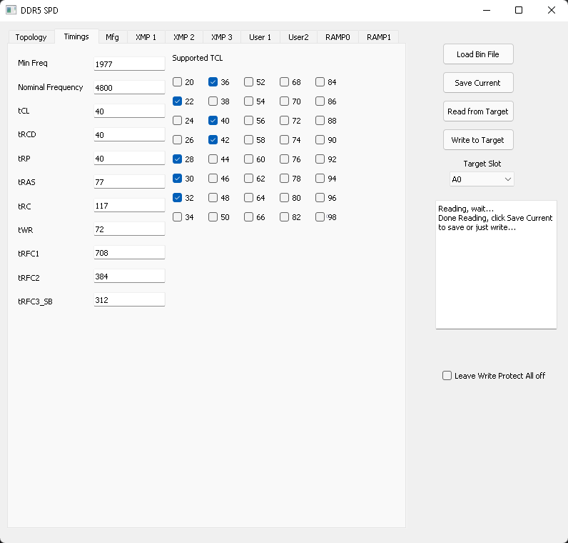
The timings according to JEDEC are also effectively standard for DDR5, with a clock frequency of at least 1996 Mbps and nominal 4800 Mbps, at timings tCL 40, tRCD 40, tRP 40, tRAS 77, tRC 117, tWR 72, tRFC1 708, tRFC2 384 and tRFC_SB 312. There are a few gaps in the supported values for CAS latency, although we have not yet been able to determine an actual functional impact in our tests.
The manufacturer information about the components is really interesting. The manufacturer of the SPD chip with the hex ID “80B3” already looks familiar from past tests. The company in question is Renesas. Although this manufacturer also has PMICs (Power Management Integrated Circuits) in its portfolio, G.Skill again chose another manufacturer for this component. “8A8C” in this case stands for Richtek.
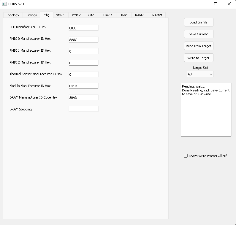
The manufacturer of the modules is of course G.Skill, which is what the “84CD” stands for here. We meet an old acquaintance at the manufacturer of the DRAM, i.e. the actual working memory ICs. Because “80AD” stands for SK Hynix. Even if the stepping or IC type cannot be read out correctly here, we can determine this relatively reliably in the early days of DDR5. Currently, Hynix only offers the 16 Gbit M-Die memory modules, which currently have the best clock potential in DDR5.
Finally, let’s move on to the XMP profile and the important related information. Of course, the PMIC type is important especially for overclocking RAM with more voltage, which is read out here as “XMP (OC) PMIC” and can thus provide more than the 1.435 V VDD and VDDQ provided by JEDEC. The recommended configuration for this kit is “1DPC” as always before with DDR5, i.e. 1 DIMM per channel.
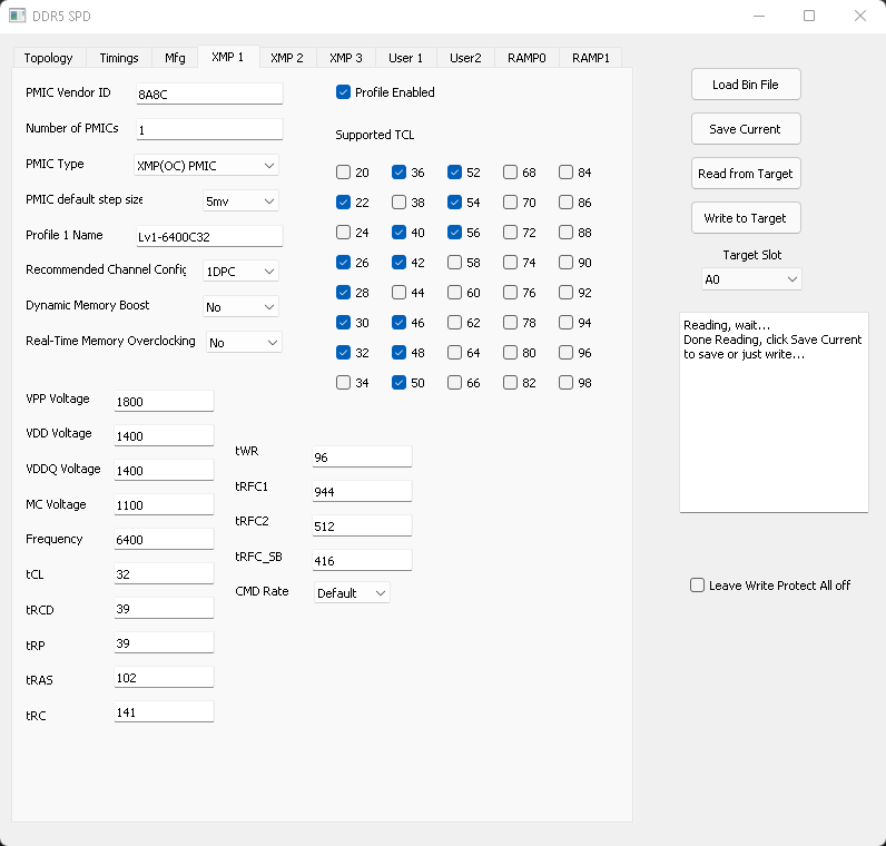
The full XMP profile at the clock rate of 6400 Mbps and thus a clock rate of 3200 MHz uses the timings tCL 32, tRCD 39, tRP 39, tRAS 102, tRC 141, tWR 96, tRFC1 944, tRFC2 512, tRFC_SB 416. The command rate is not fixed. For the voltages, G.Skill specifies 1800 mV for VPP, as well as 1400 mV each for VDD and VDDQ and 1100 mV for VDD2 (MC Voltage).
Heatsink test
As usual in our RAM tests, the modules have to really sweat with a loaded XMP profile. The RAM stress test Testmem5 v0.12 with profile “Extreme1@Anta777” is used for this due to its extremely high heat load for the working memory. The temperature is recorded with type-K probes on the module with the memory ICs on the inside, logged at 0.5 second intervals, forming the delta to the room temperature.
On the one hand, we can test whether the modules are actually stable in XMP mode, and on the other hand, we gain an initial indicator of the cooler’s performance and the associated thermal potential for further overclocking. We test the modules once completely passively without any further cooling and a second time with a 2000 rpm 120 mm fan directly on the modules.
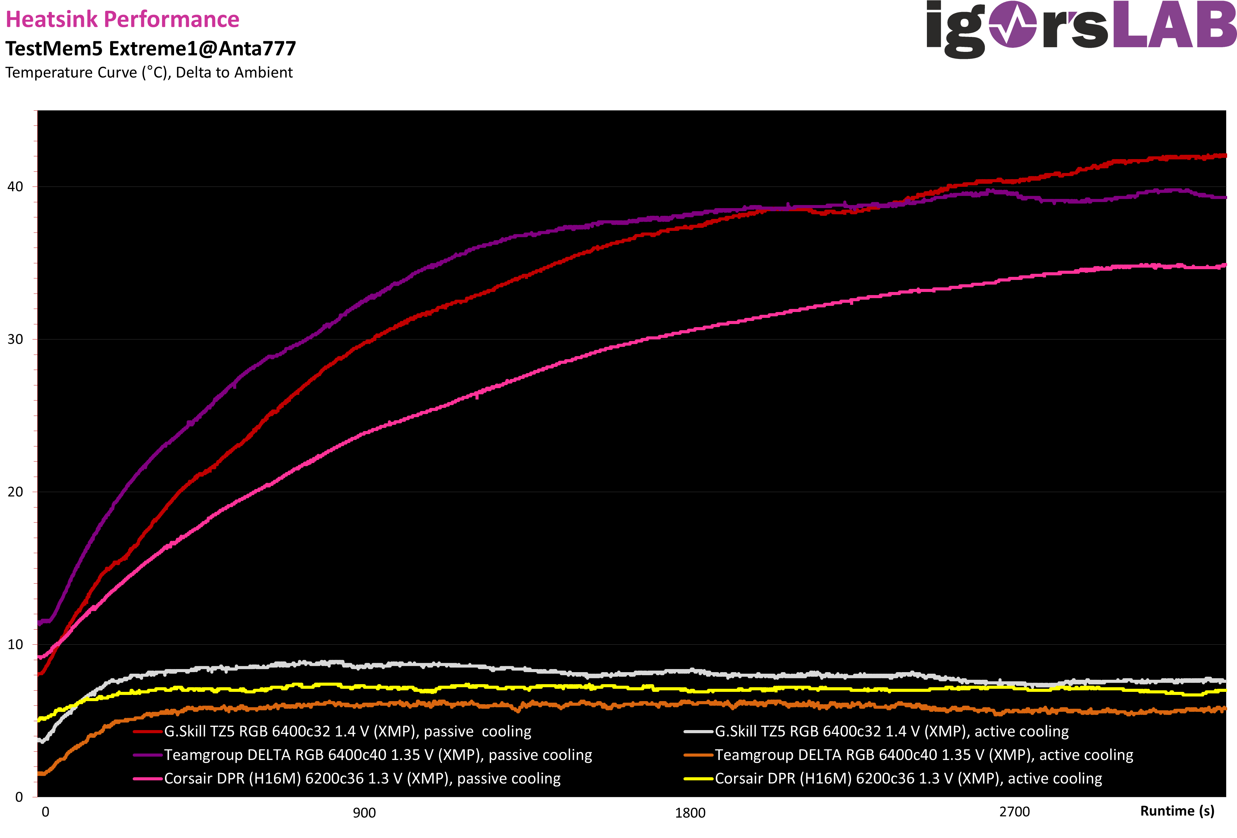
The G.Skill Trident Z5 modules with their higher thermal mass can initially stay cooler in passive mode than the recently tested models from Teamgroup, but then they are nevertheless heated up to more than 40 °C above room temperature by the 1.4 V of their XMP profile after about 30 minutes. In passive mode, the gaps are smaller, but the Trident Z5 sticks are still the warmest. However, considering the 50 and 100 mV lower voltages of the other modules plotted here, G.Skill still doesn’t have to hide at all with the performance of their coolers.


14 Antworten
Kommentar
Lade neue Kommentare
Urgestein
Veteran
Mitglied
Urgestein
Veteran
Urgestein
Urgestein
Urgestein
Urgestein
Urgestein
Urgestein
Veteran
Neuling
Neuling
Alle Kommentare lesen unter igor´sLAB Community →