


Tear Down in the video
Since I now also run my own YouTube channel at many request, I also made a detailed video for this map for the Tear Down and also explained the most important measurements. The text here is of course much more detailed, but for a better understanding (also of the following pages) the video is certainly the right appetizer:
Board analysis
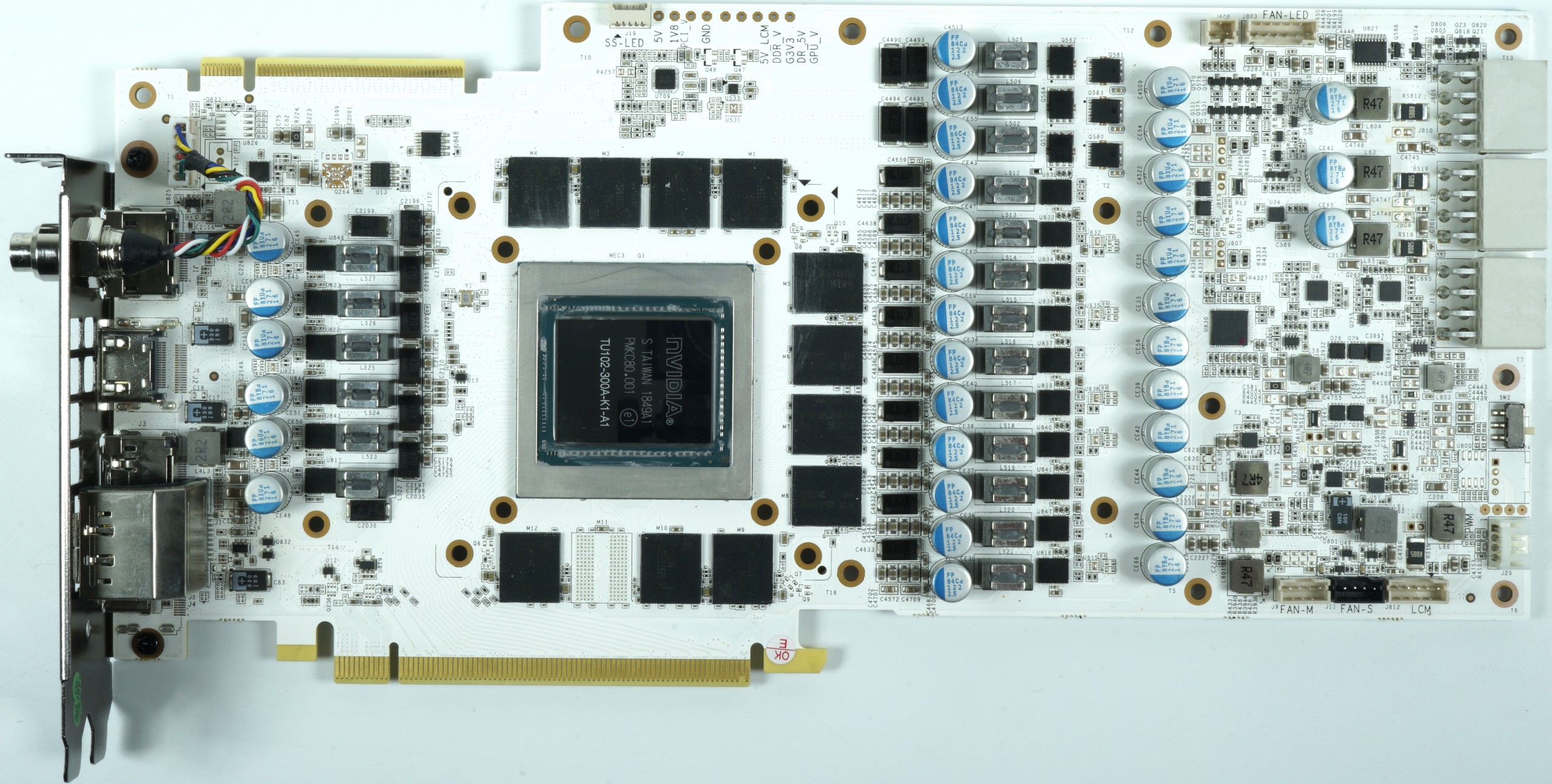
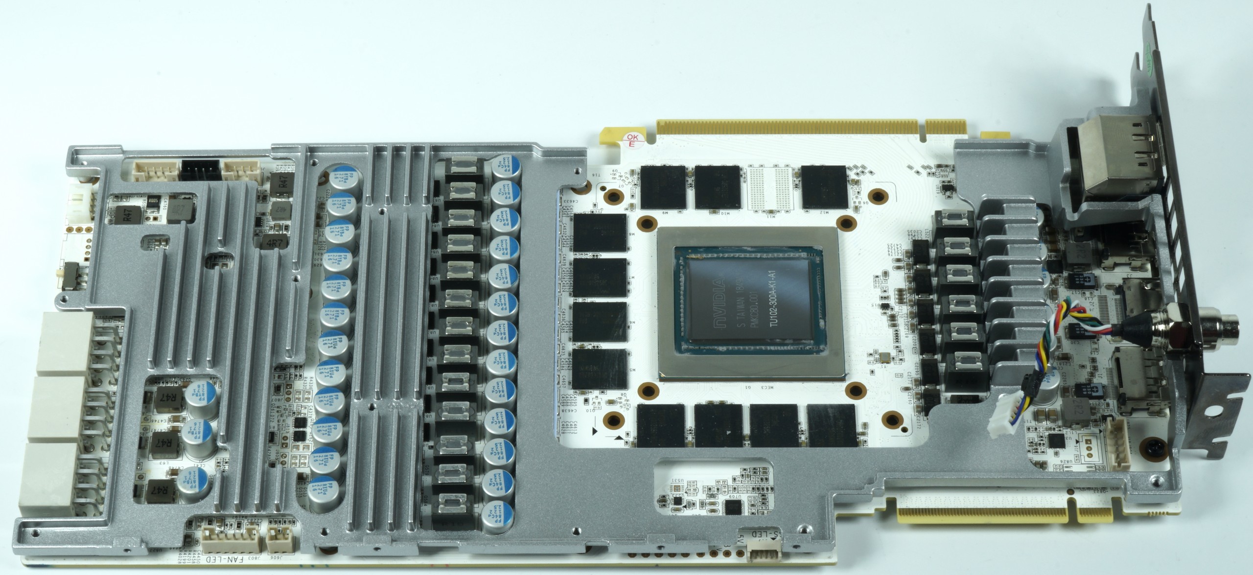
A very striking feature are the three thick 8-pin ATX power supply connections, although considering the high power limit of 450 watts, one can't help but notice. In addition, each rail has a shunt, as well as a 330 mH coil with capacitor as a complete LC link for smoothing. But later on more in the power consumption and the zoom recordings of the power consumption, especially with the maximum OC.
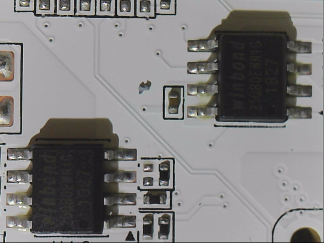
Despite the changed design, the board still looks quite tidy, although this is not really a feat with the sheer size of the board. In addition, however, the clip connector for the OLED display was visibly implemented, as well as the voltage taps for measurement purposes in the extreme OC (top center). In addition, two, instead of just one EEPROM, are eye-catching for the two switchable BIOSes.
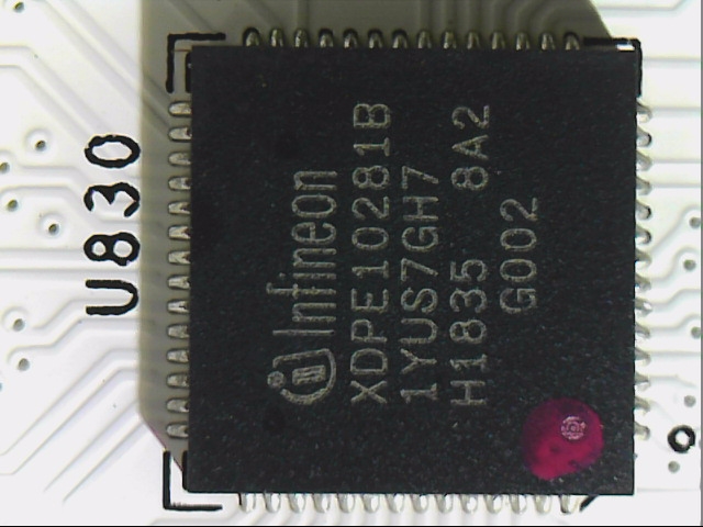
But let's start with the power supply. Let's start with phase splitting. A completely new chip from Infineon in the form of the XDPE10281 takes over the task of the PWM controller, which was specially developed for the provision of high-precision output voltage systems for the latest generation of GPUs. The integrated SMBus interface offers enough flexibility to optimize performance and efficiency and also to connect the right software
The chip is so new that even the data sheets were and are under NDA. Ok, not for us, because I have some information about it for you. It is a very special dual-rail controller of the latest generation, which means that it can control suitable power stages directly and even two parallel simultaneous lyses. External phase multipliers or gate drivers are no longer needed. This chip may have been installed on a graphics card for the first time in the form of this board.
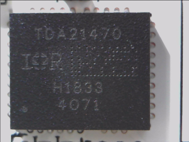
It also has programmable output voltage and active voltage positioning functions to adjust the output voltage depending on the load current, so that it is optimally positioned for a good load current transition. It also supports NVIDIA Open Voltage Regulator Type 4i+ with PWMVID function. The PWMVID input is buffered and filtered to create a very accurate reference voltage. The controller supports, as just written, special smart power stage chips (PLCs) that rely on a more accurate MOSFET DCR in real time instead of the inaccurate Inductor DCR. This TDA21470 from International Rectifier (now part of Infineon) used here provides very accurate information about e.g. currents (IMON) and temperatures (TMON).
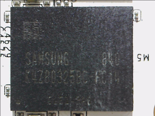
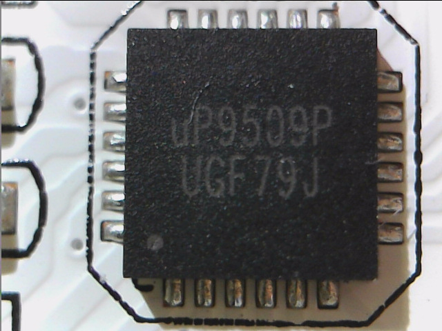
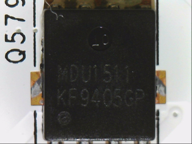
We count a total of 16 voltage converter circuits for the GPU. However, since you rely on a neat 8-phase design, a total of eight real phases are double-connected. The three phases for memory are generated by a simpler uP9509 from UPI in true 3-phase mode, where three discrete voltage converters are equipped with one MDU1514 each on the high-side (66.3 A) and a MDU1511 (100 A) on the low-side. The coils are a custom-made taiwanese manufacturer, which I am sorry not to mention.
All this is completed by a dual BIOS with DIP switch and I really recommend the linked video for accurate board analysis. Because that's where I go into the details.
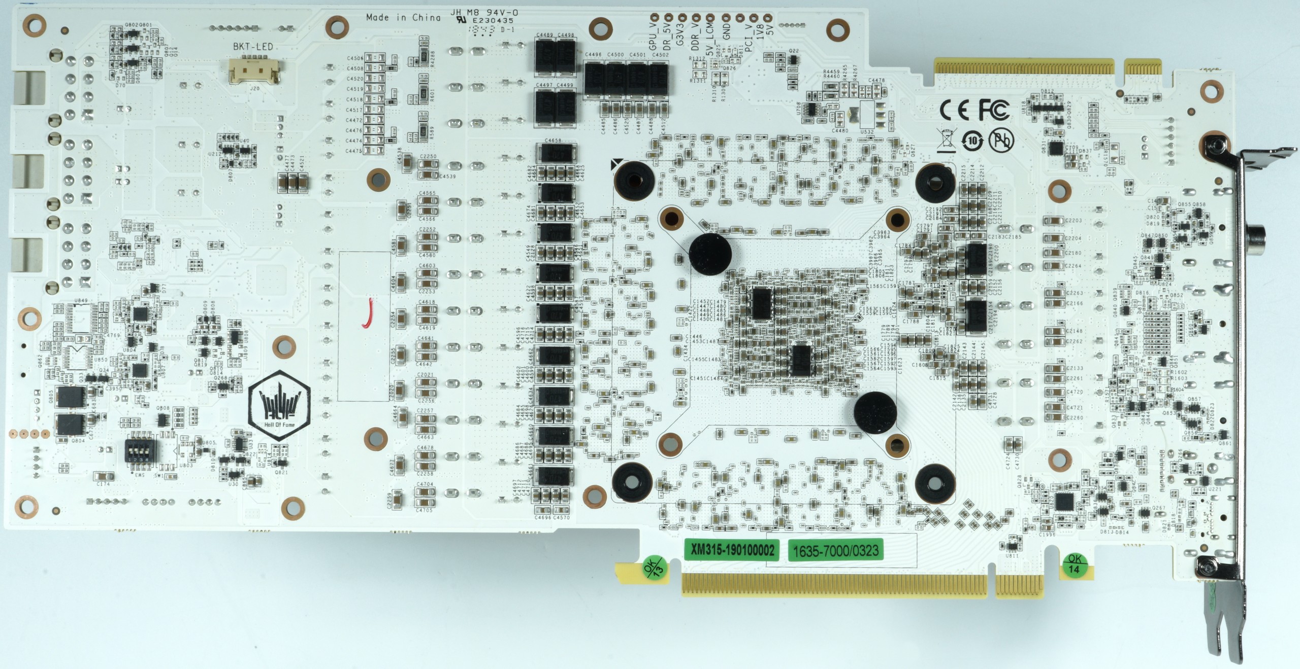
The back is free of secrets and also looks quite tidy. If you would like to find out more details about this type of power supply and the improvements at Turing, please refer to our Investigative Article "Nvidia GeForce RTX 2080 Ti – Internal Details on Power Supply, Deviating Components and Where the Spikes which is always worth reading. There you will also learn more about the new Smart Power Stages, which replace the traditional, individual VRMs. The following table contains the most important components:
GPU Power Supply |
||
|---|---|---|
| PWM Controller | XDPE10281B Infineon 8-phase/16 circles |
 |
| Gate Driver | integrated, not external | |
| Vrm | 16x TDA21470 International Rectifier/Infineon Smart Power Stage |
 |
| Coils | Encapsulated Ferrite Choke | 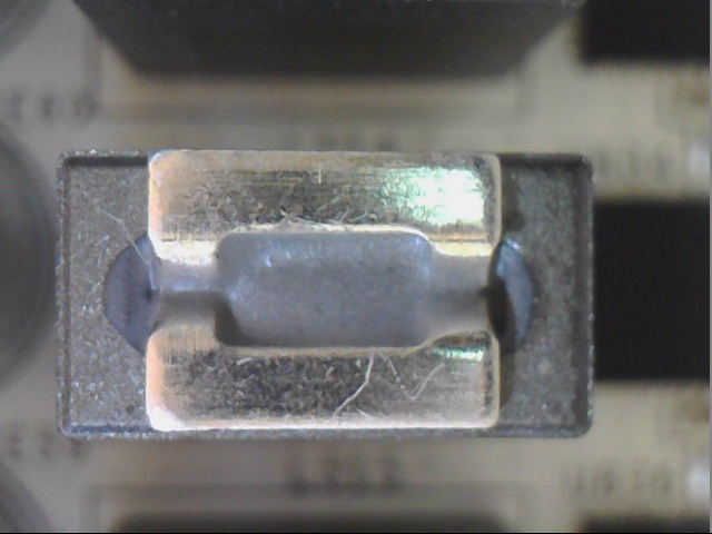 |
Memory and power supply |
||
| Modules | K4Z803258C-HC14 Samsung 8x 8GB GDDR6 SGRAM Modules 2 Channels x 256 Meg x 16 I/O 2 Channels x 512 Meg x 8 I/O 14Gb/s |
 |
| PWM Controller | uP9509 UPI Semiconductor 3 phases |
 |
| VRM High-Side |
3x MDU1514 Magna Chip Single-N-Channel Trench MOSFET |
 |
| VRM Low-Side | 3x MDU1511 Magna Chip Single-N-Channel Trench MOSFET |
 |
| Coils | Encapsulated Ferrite Choke | |
Other components |
||
| Controller | 8-bit ARM Controller | 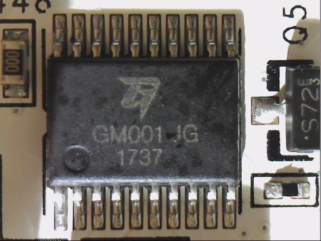 |
| BIOS Switch | DIP Switch | 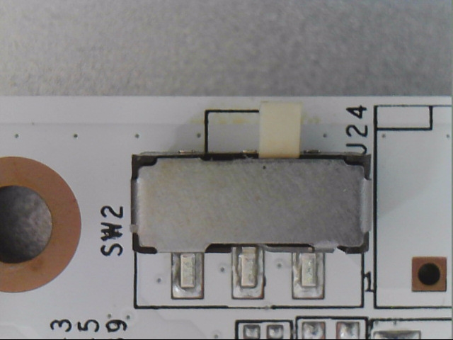 |
| Eeprom | 25Q8x Winbond EEPROM Dual BIOS |
 |
| Shunts | 1x coil + capacitor (LC smoothing) and shunt per 12V rail (4) |  |
More details |
||
| Other Features |
– 3x 8-pin PCI-Express connectors for power supply – Complete LC links in the entrance area |
|
Cooler and backplate in detail
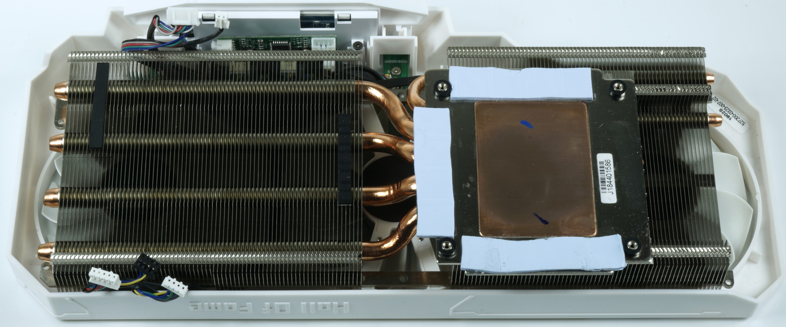
The actual radiator structure alone weighs well over 1000 grams, including the cover and fans. Four thick 8 mm heatpipes and a circumferential 6 mm heatpipe for the GPU block then distribute the waste heat from the GPU heat sink to the cooling fins. As always, KFA2 uses a fan arrangement with three 8.7 cm fans above the cooling frame.
A more detailed impression including further details can be provided in the detailed video with the cooler tear-down.
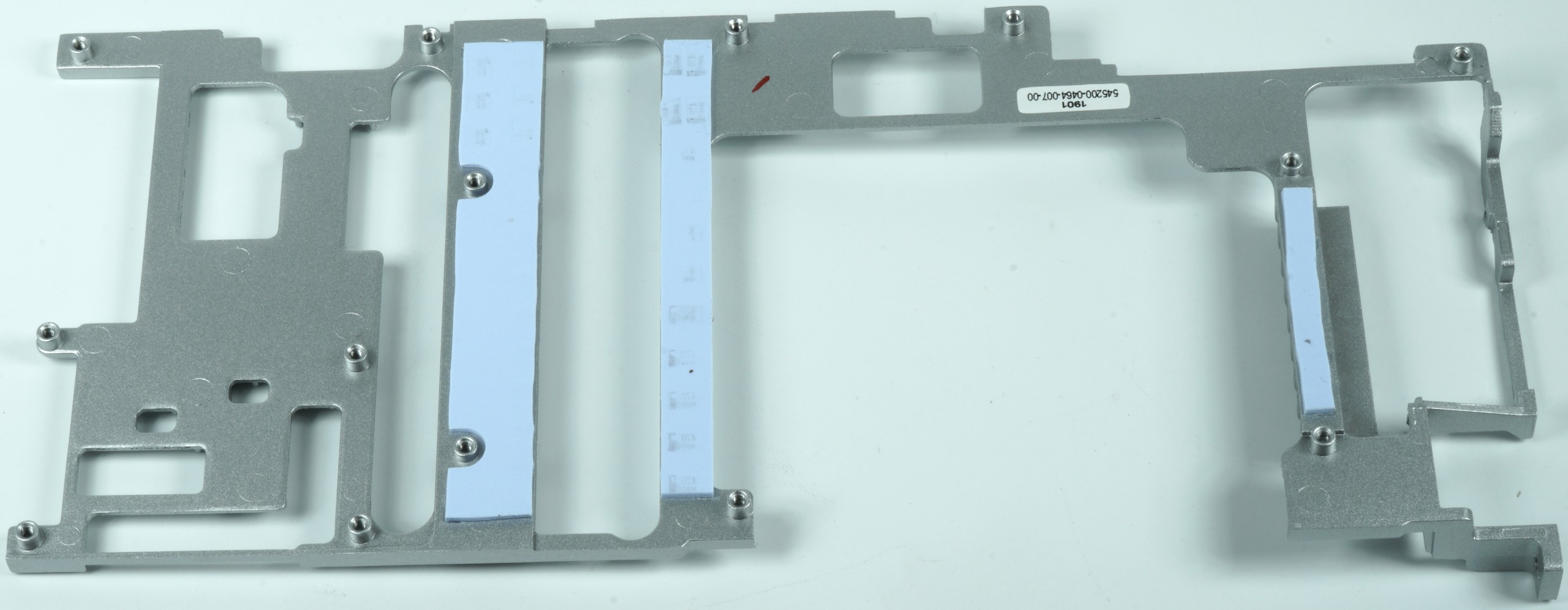
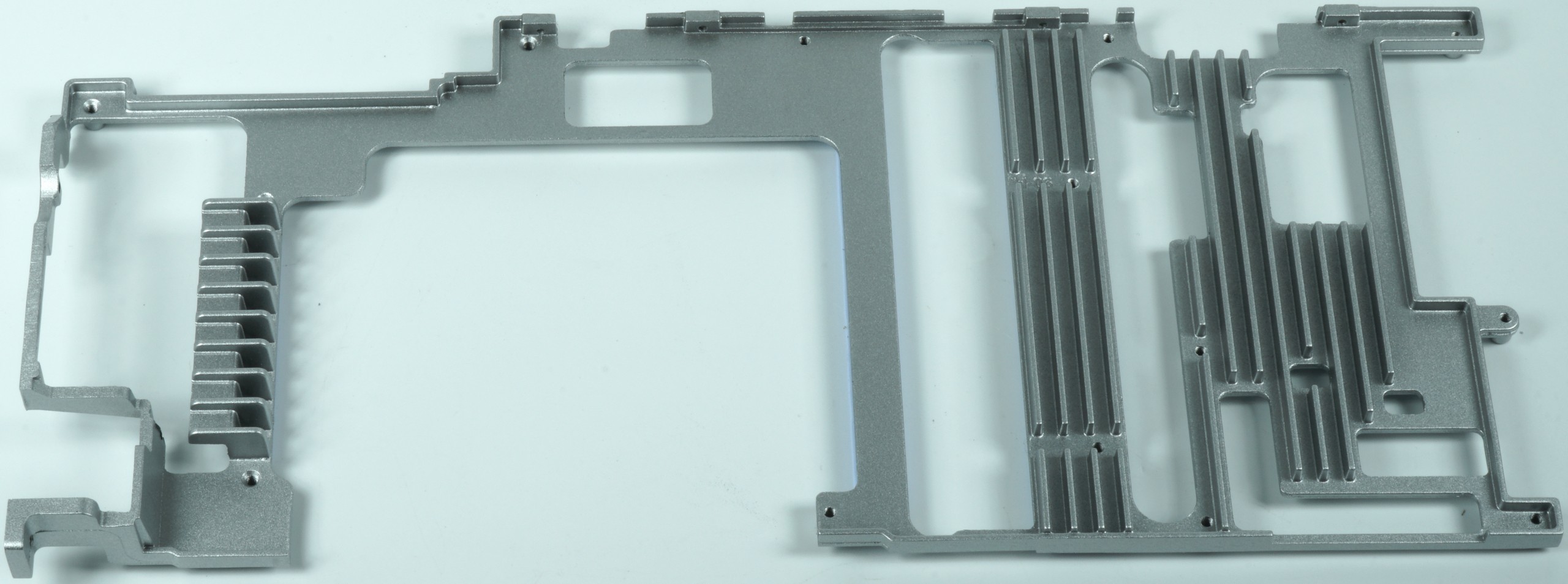
A large cooling frame permanently blown by the three fans as aluminium casting additionally stabilizes the board and ensures the cooling of the memory and the voltage converters. Galax also relies on high-performance, 1 mm thick thermal guide pads.
In contrast to the Lightning Z from MSI, the range around the six individual voltage converter circuits (right) can be completely convincing, whereby the cooling performance of this sandwich solution is surprisingly confident. That's what you have to do first. But more on that later.
The white printed aluminium backplate has no cooling function. It's a pity, but hardly necessary anyway, as we'll see. The cooling system briefly summarized in a tabular overview:
| Cooling system at a glance | |
|---|---|
| Type of cooler: | Air |
| Heatsink: | Copper Heatsink, GPU |
| Cooling fins: | Aluminum, horizontal alignment related |
| Heatpipes | 4x 8mm, 1x 6 mm, copper composite |
| VRM cooling: | 16 GPU Power Stages via cooling frame 3 Memory VRM via cooling frame |
| RAM cooling | via frame on the GPU heatsink |
| Fan: | 3x 8.7 cm fan, 11 rotor blades semi-passive lyrised |
| Backplate | Aluminum, no cooling function |


Kommentieren