


Ryzen has been known to be a gluey matter since Zen 2, though not in a conventional way. AMD has been combining CCX chiplets with IO chiplets into one CPU since the Ryzen 3000 series and the glue is the package in the form of copper and fiberglass. Today, we are seperating the glued components of two such CPUs and glueing them back together to form a new one – at least virtually – which could theoretically soon be available in stores.
Premise and theory
Although the chiplet concept was initially ridiculed by competitors and labelled as a cheap alternative to the conventional monolithic construction method, the advantages of the better usability and combinability of the chiplets could not be denied. Unsurprisingly, the trend has caught on in the industry, both in the last 3 generations of Ryzen CPUs, but Intel has also adopted some of these principles in its latest product families in the server, desktop and mobile segments. …evil tongues might even say copied.
Today’s article is aimed at the combinability of various chiplet components, because if they can be swapped between products so relatively easily, with a little extrapolation we can also infer the theoretical performance of such speculative products. And if we look a little into the past, then such relatively simple forecasts have largely come true. So today we dare to take another such look into the milkmaid’s crystal ball and consider what we might expect in the future with Ryzen 6000.
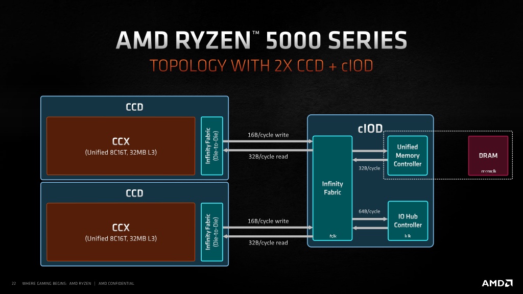
With the Ryzen 5000 generation and the Zen 3 architecture released, AMD has made a big leap in terms of compute chiplet (CCD/CCX) performance, the ones that the CPU cores and cache sit on. However, the IO chiplet (cIOD, IO-Die) still uses the same design as with Ryzen 3000, based on a 12 nm process, while the compute chiplets are already manufactured with the newer 7 nm process. Accordingly, it would be relatively obvious to assume that AMD will probably start right here for the next generation of CPUs, leaving the compute chiplets mostly identical and prioritizing a new IO chiplet as an upgrade to achieve more performance.
Conveniently, there are already CPUs on the market with such a new design of the IO portion, in the form of Ryzen 4000G Pro APUs. Here, both Zen 2 CPU and Radeon GPU are installed on a monolithic chip, mainly because the GPU part would react very sensitively to possible higher latencies of a chiplet architecture. So AMD was forced to put all the components of the APU on a single piece of silicon and include the IO chiplet. Accordingly, the opportunity has been taken to re-engineer the IO portion to achieve better performance there with higher clock speeds and tighter timings.

So already today we can compare this Ryzen 7 4750G Pro CPU, based on older Zen 2 compute chiplets but with new IO portion, with a Ryzen 9 5950X CPU, based on Zen 3 compute chiplets but with older IO die. Finally, we can take the best of both worlds and mathematically calculate what the memory performance of a CPU with Zen 3 compute chiplets and new IO chiplet would approximately be. As a reference for that calculation we use the DDR4-3800 performance, to which the respective percentage performance gain of the faster clock rates, made possible by the new IO portion, are added.
Test hardware and methodology
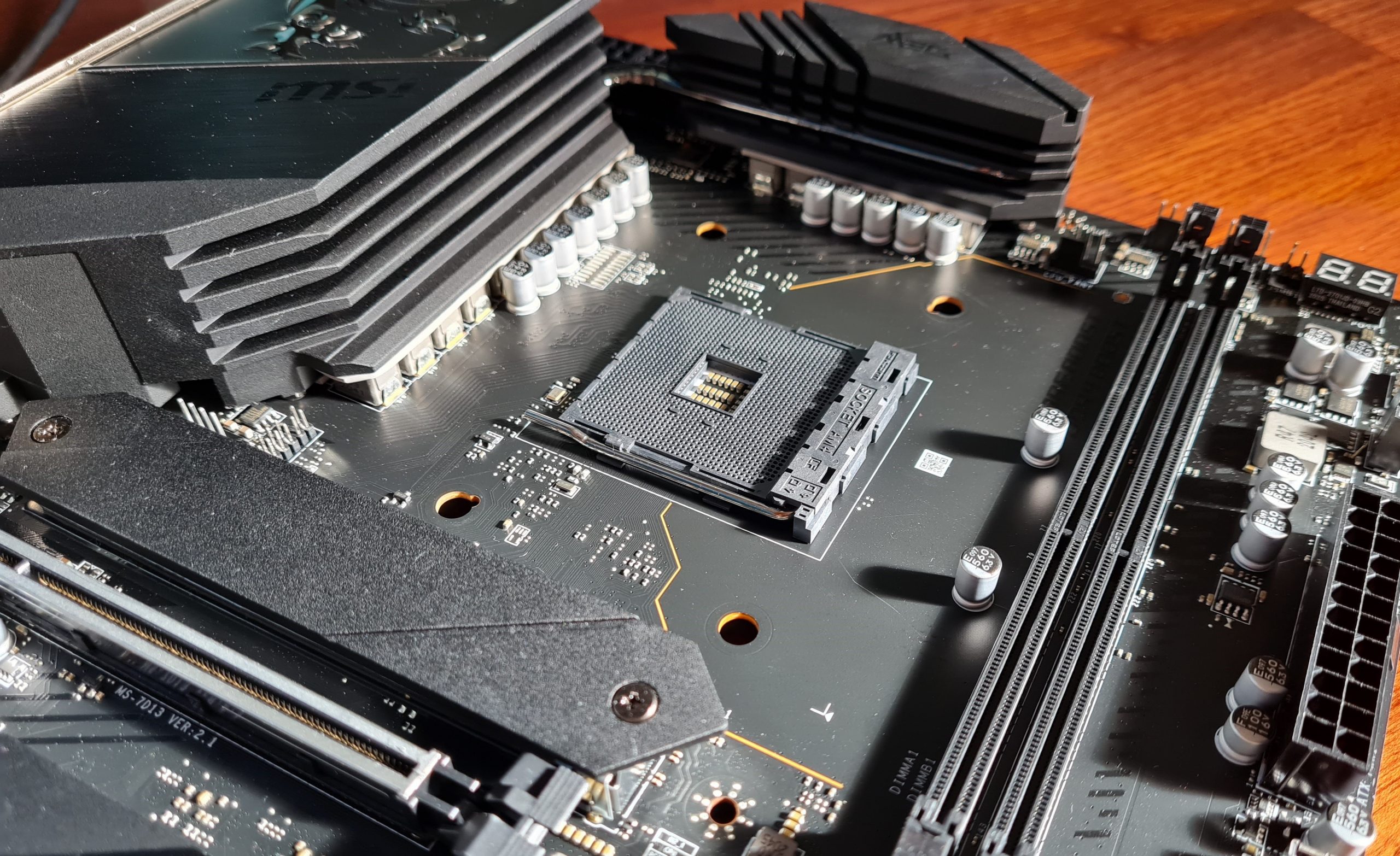
The MEG B550 Unify-X motherboard, which was kindly provided to us by MSI, serves as the basis for the test. With this board the focus is on the maximum performance of CPU and RAM, which is also why there are only 2 DIMM slots. Everything that has no meaning for the performance, such as RGB lighting and other bells and whistles have been removed. This makes it perfect to compare the memory performance of two CPU generations without having to expect a bottleneck on the part of the board.
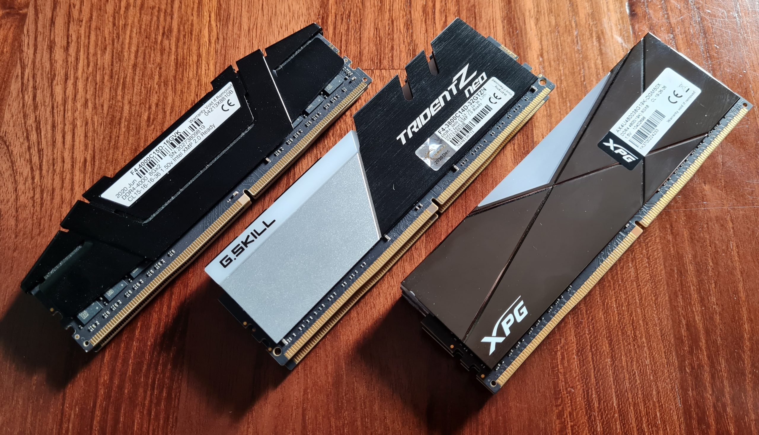
Our selection of memory kits and clock rates is also correspondingly high-end. A Sinlge-Rank 2x 8 GB kit and a Dual-Rank 2x 16 GB kit, each based on Samsung 8 Gbit B-Die, and a Single-Rank 2x 8 GB kit based on Hynix DJR are tested. The following clock rates and timings are tested with them:
- Single-Rank DDR4-3800 1:1 CL14-14-14-28, tRC 42, tRFC 300, Vdimm 1.5 V
- Single-Rank DDR4-4533 1:1 CL16-16-32, tRC 48, tRFC 300, Vdimm 1.5 V
- Single-Rank DDR4-5200 2:1 CL20-27-27-47, tRC 78, tRFC 600, Vdimm 1.6 V
- Dual-Rank DDR4-3800 1:1 CL14-14-14-28, tRC 42, tRFC 300, Vdimm 1.5 V
- Dual-Rank DDR4-4533 1:1 CL16-16-32, tRC 48, tRFC 300, Vdimm 1.5 V
In the following, Single-Rank is abbreviated with “SR” and Dual-Rank with “DR”, the “DDR4-” prefix is omitted for the clock rates and only the CAS latency is specified for timings and voltage in order to achieve better readability. Only the DDR4-3800 settings could be tested with both CPUs, due to limitations of the infinity fabric and memory controller of the 5950X. All tested settings were checked for stability with a run of Testmem5 “Extreme1@Anta777”, so they are really representative for the performance in daily use.
You might think at first that such high clock rates would not be achievable for most users anyway. But today’s high-end is tomorrow’s mid-range, as we all know, and the settings used were just clock speed, primary timings, tRC, tRFC, and RAM voltage (Vdimm), so this would pretty much match an XMP usecase. That’s also all a mainboard usually does when loading an XMP profile. Thus, the measured performance would actually be achieved by the user of tomorrow with a mid-range mainboard without much effort.
The following is a complete list of the test hardware used:
| Test system | |
|---|---|
| Hardware: |
|
| Cooling: |
|
| Housing: |
|
| Periphery: |
|


24 Antworten
Kommentar
Lade neue Kommentare
Mitglied
Urgestein
Mitglied
Urgestein
Urgestein
Urgestein
Urgestein
Urgestein
Urgestein
Veteran
Urgestein
Urgestein
Neuling
Urgestein
Urgestein
Urgestein
Urgestein
Mitglied
Alle Kommentare lesen unter igor´sLAB Community →