


Interior structure
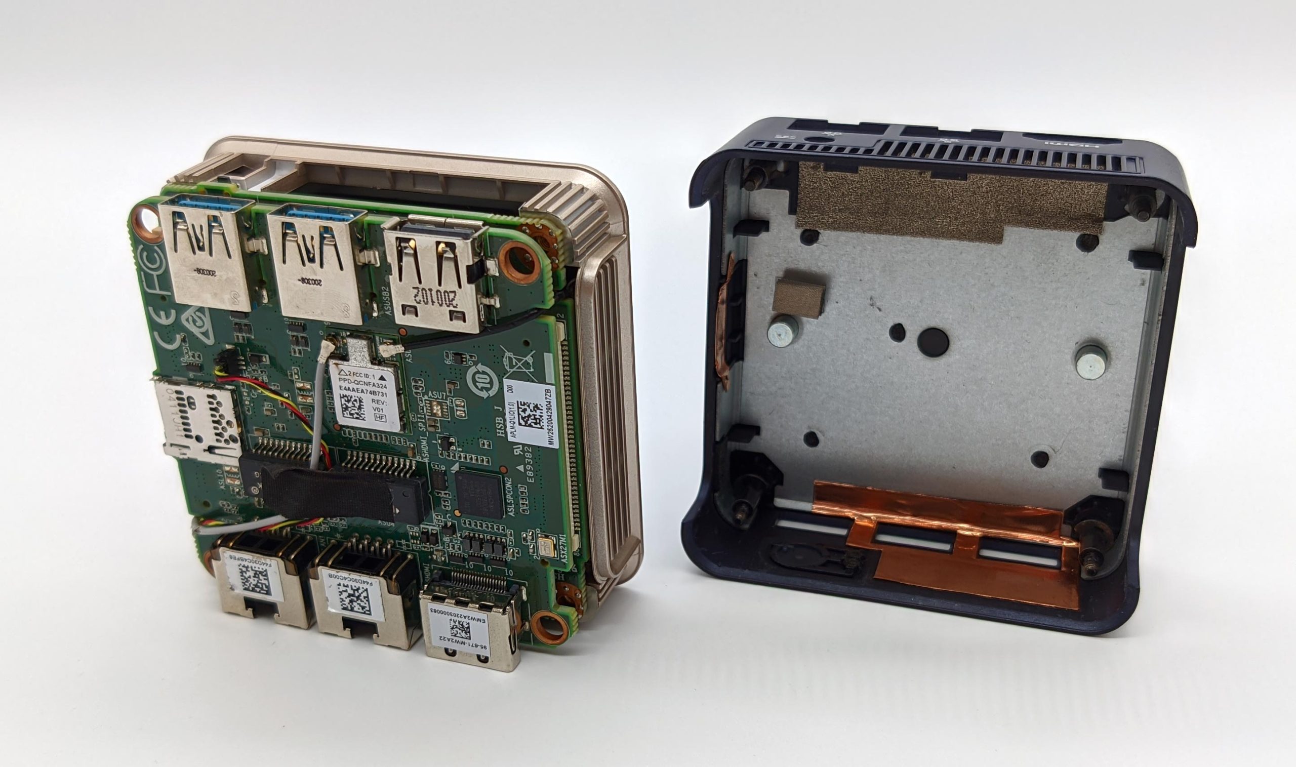
If you remove the four screws on the underside of the system, which were clearly visible earlier, you can open it carefully. The case splits into its two colored parts, with the PCB still attached to the upper part.
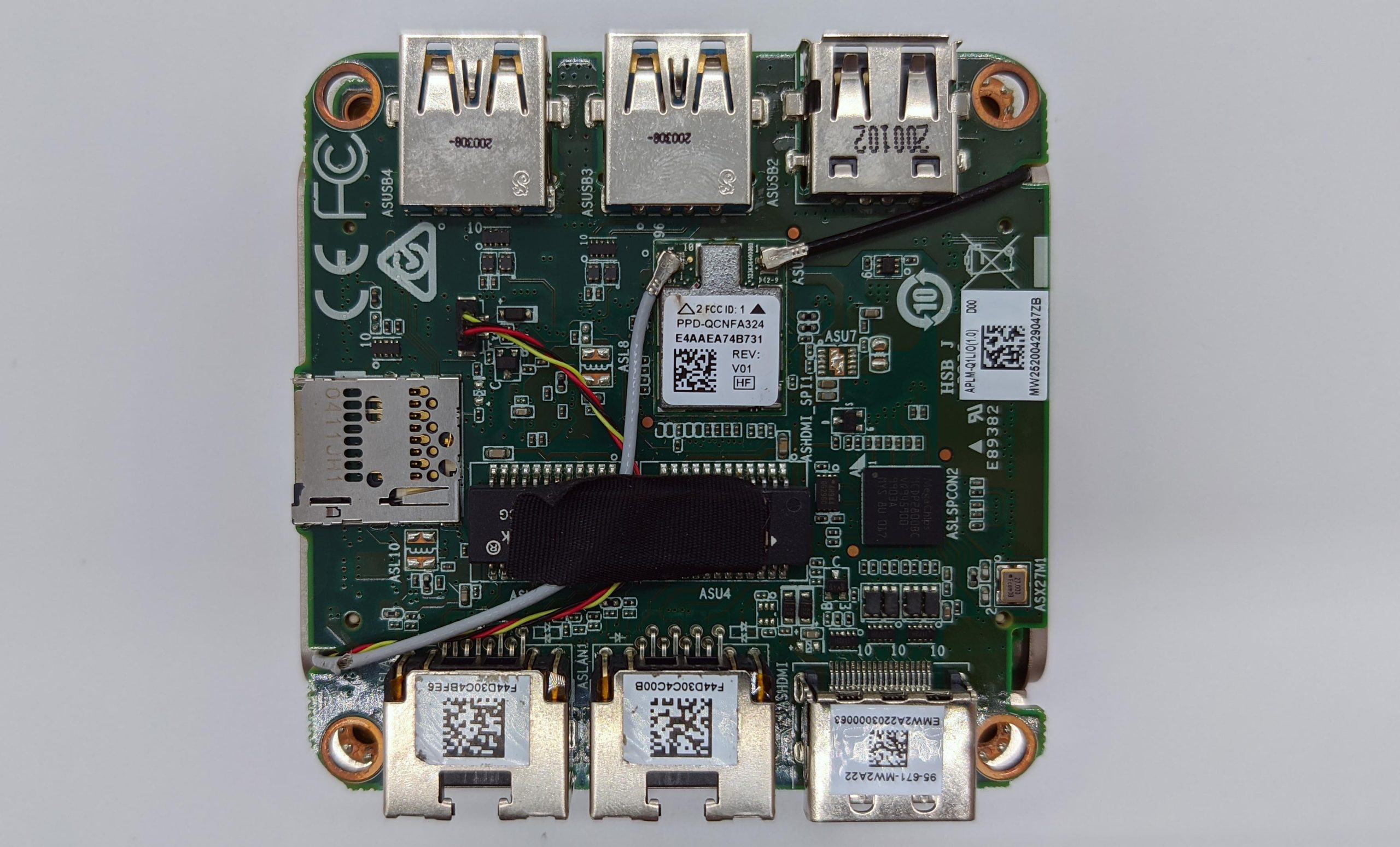
A Qualcomm Atheros QCNFA324 chip in the center is responsible for WLAN 802.11 ac/b/g/n and Bluetooth 4.1. On the right of the picture is a DisplayPort 1.2a to HDMI 2.0 converter chip, an MCDP2800 from kinet-ic.
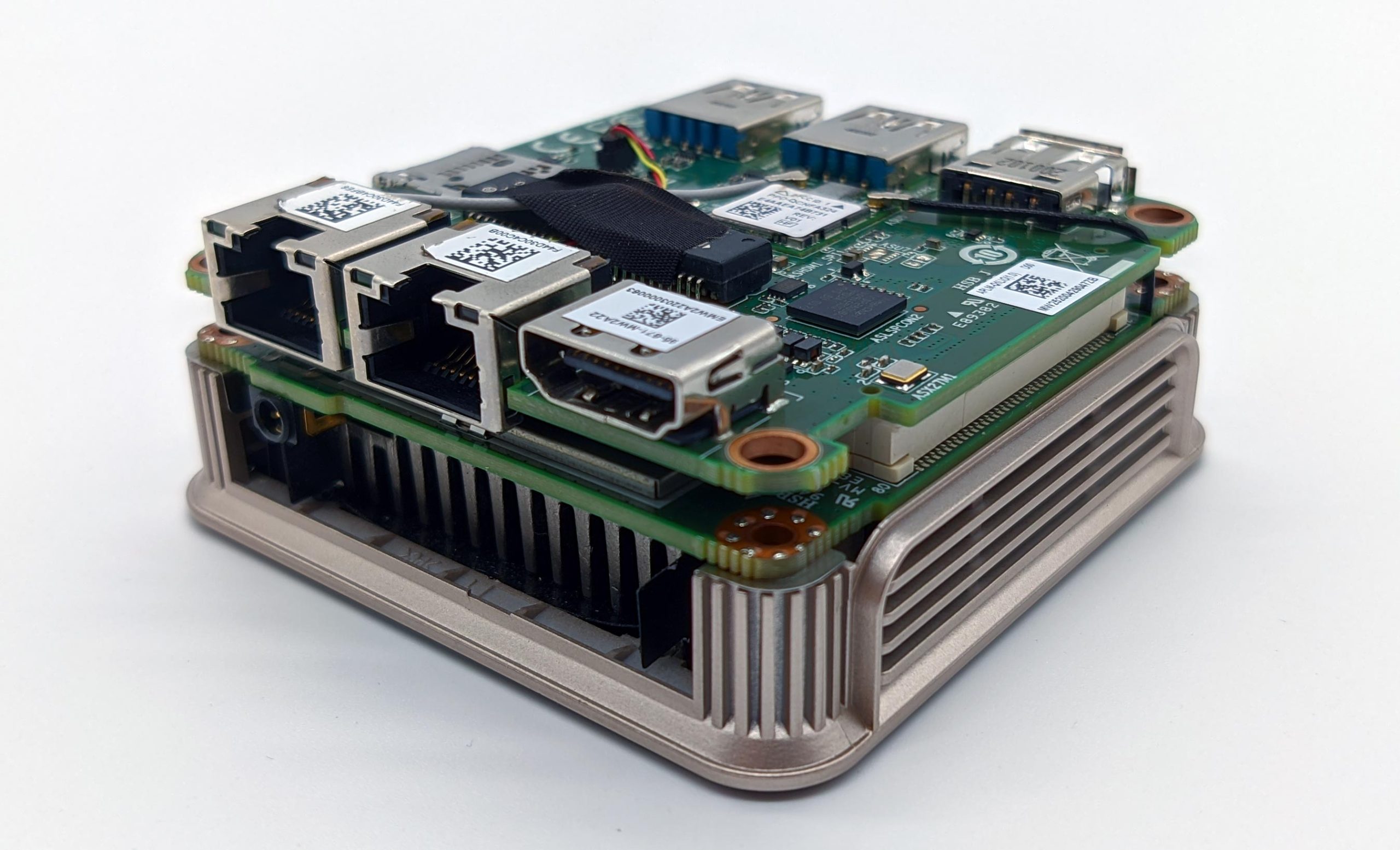
What surprised me a bit is the sandwich design here with two separate PCBs that are connected via wide connectors. Here, in the side view, you can already see something of the cooling fins of the equally small cooling solution.
Unfortunately, it was not possible for me to completely disassemble the system and also photograph the board with the CPU due to the cables of the WLAN and fan. With such delicate small parts, I didn’t want to take the risk of damaging something.
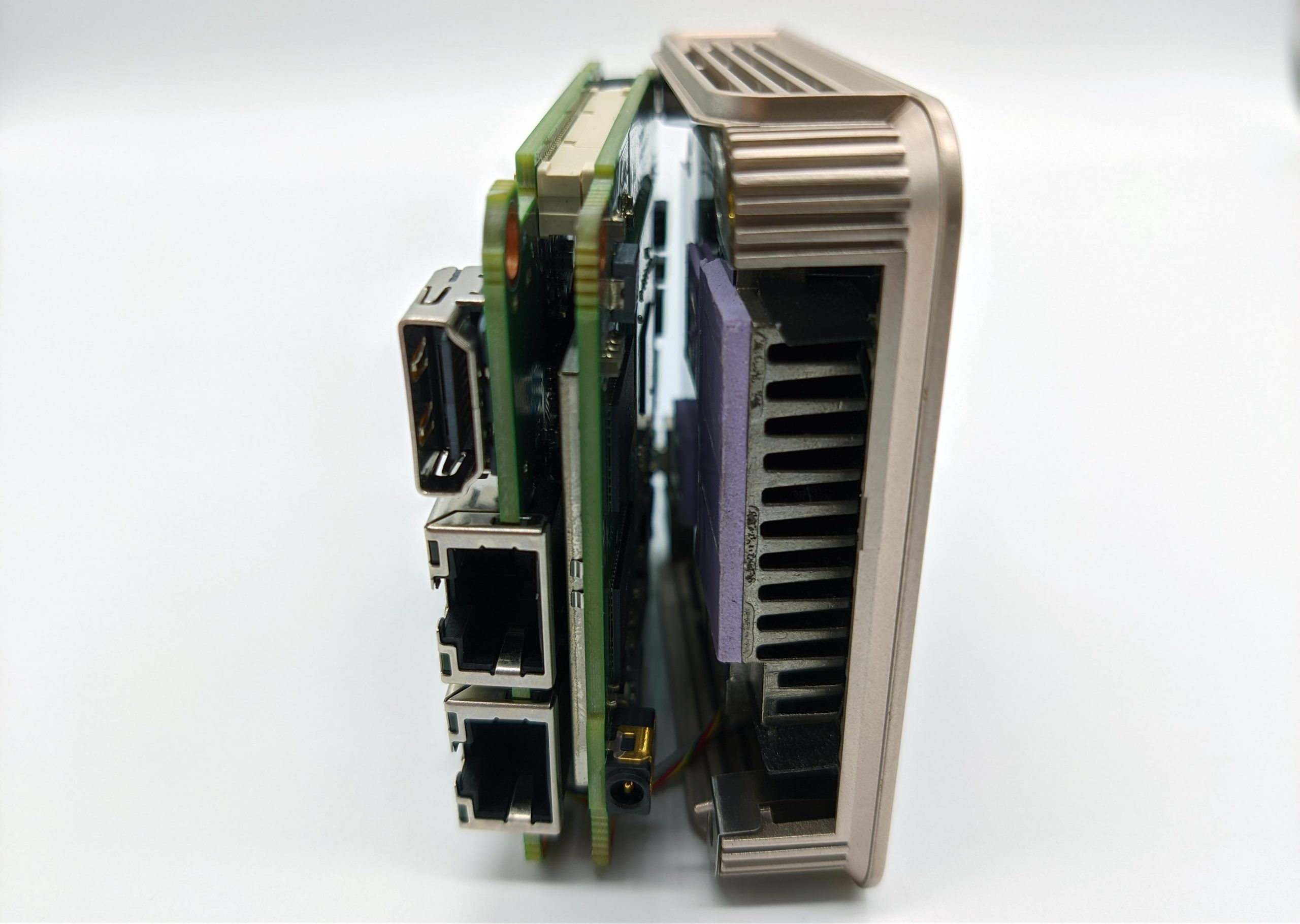
Nevertheless, I tried to take a few pictures through the narrow gap. The processor and a few surrounding parts are connected to the heatsink with their own heat conduction pads, classic heat conduction paste is not used.
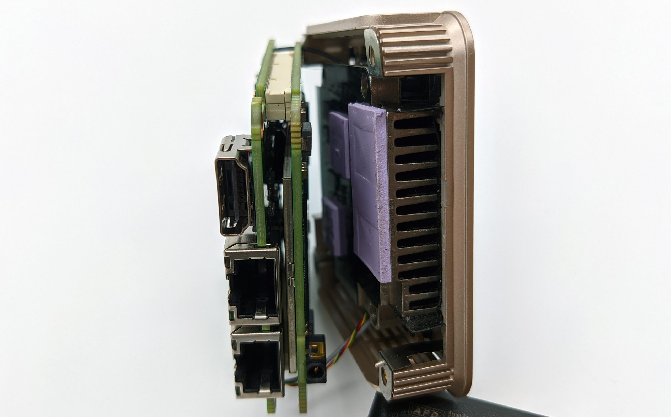
For the parts that are cooled away from the CPU, I would guess the soldered-on RAM and eMMC memory modules.


13 Antworten
Kommentar
Lade neue Kommentare
Veteran
Urgestein
Neuling
Urgestein
Urgestein
Moderator
Urgestein
Urgestein
Veteran
Moderator
Veteran
Mitglied
Moderator
Alle Kommentare lesen unter igor´sLAB Community →