


For the teardown of the modules, I use my conventional hairdryer as usual, which doesn’t work as well as with some other RAM modules. The reason for this is the disproportionately strong adhesive that attaches the two cooler halves and resists removal like a mixture of concrete and chewing gum, especially on the side without memory chips. Unlike the DDR4 modules we tested before, I don’t give up so easily today and after about an hour, both cooler halves are removed from the board. Two of the RGB LEDs were torn off during the procedure, but they could be soldered back on afterwards and work again.
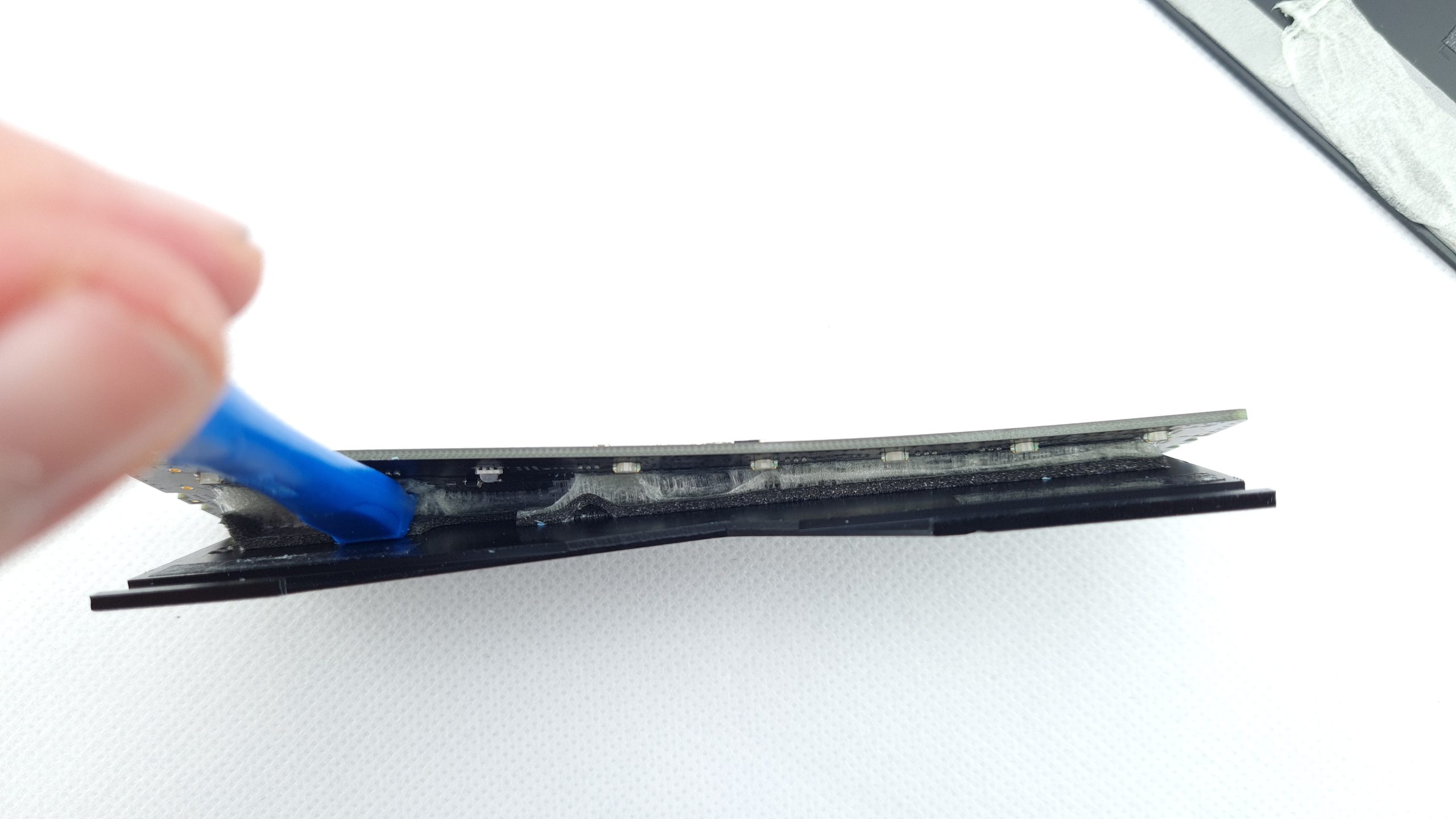
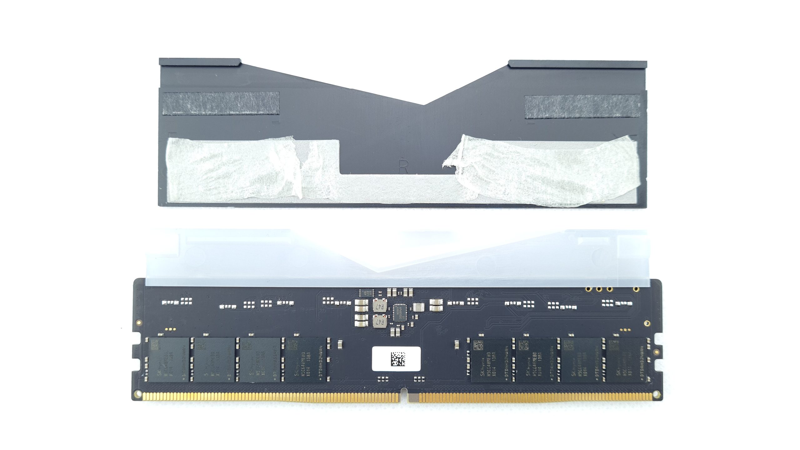
Unfortunately, the removal of the cooler does not leave the adhesive strips unscathed, which dissolve into several pieces. Although the modules can be reassembled this way without measurable influence on the cooling performance, you probably would not want to go through this glue odyssey too often. The construction of the heatsinks is solid, but unfortunately only the memory chips are cooled, not the PMIC. The latter is responsible for the voltage conversion from 5 V to partial voltages of DDR5 and is thus also a heat source that should not be neglected. Although this component is designed for well over 100 °C, it should not experience any disadvantage in terms of service life, but its waste heat is released into the board and thus causes higher temperatures of the ICs and potentially slightly earlier, heat-related instability.
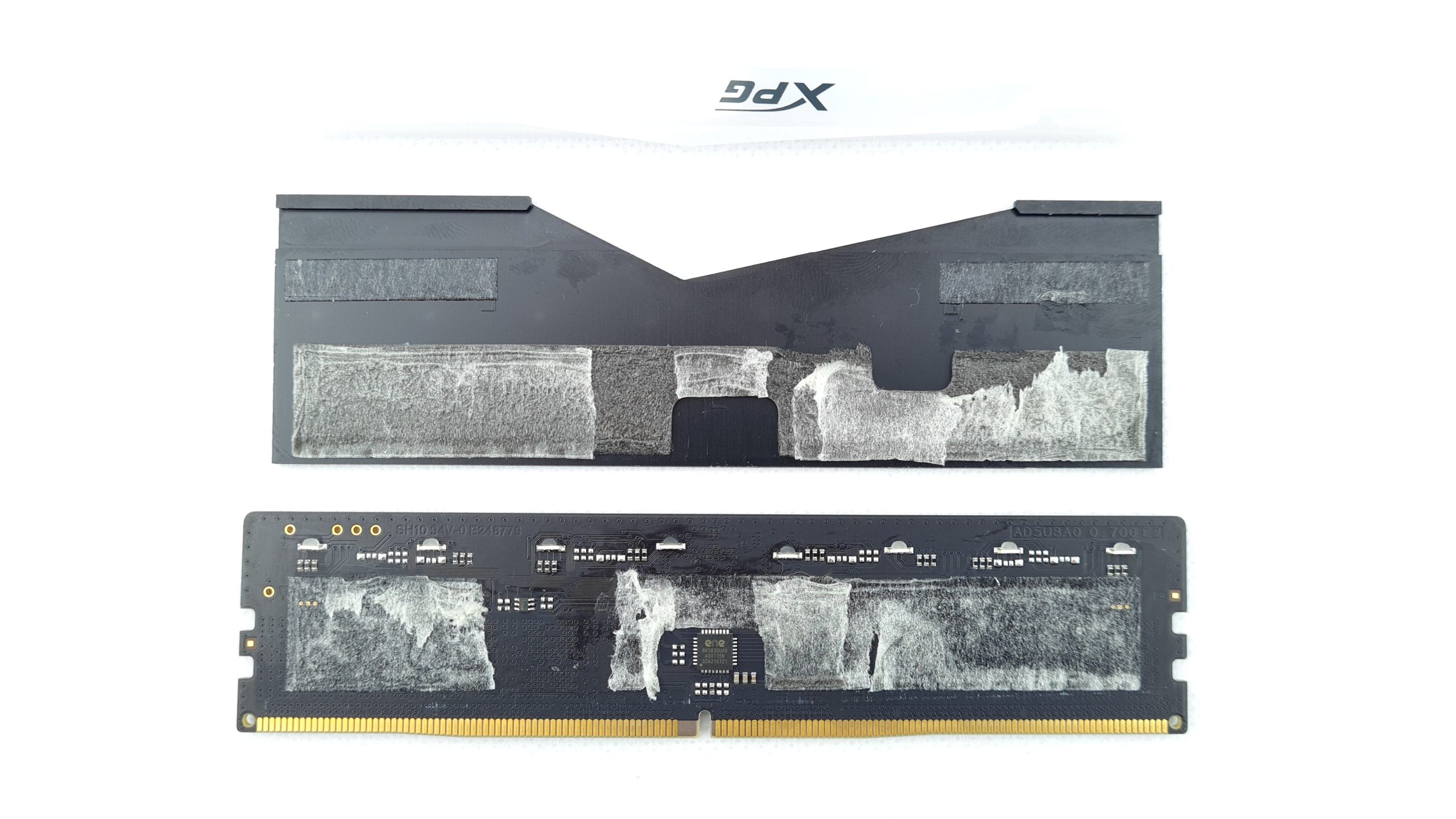
On the back, the board is stamped “SH10 94V-0 E248779” and “AD5U8A0 0 . 700 E2”, whereby the latter should indicate the production type of the board due to the A0 part as PCB layout. However, I cannot name the manufacturer or OEM based on this. As always, if you have any tips here, feel free to let me know in the forum.
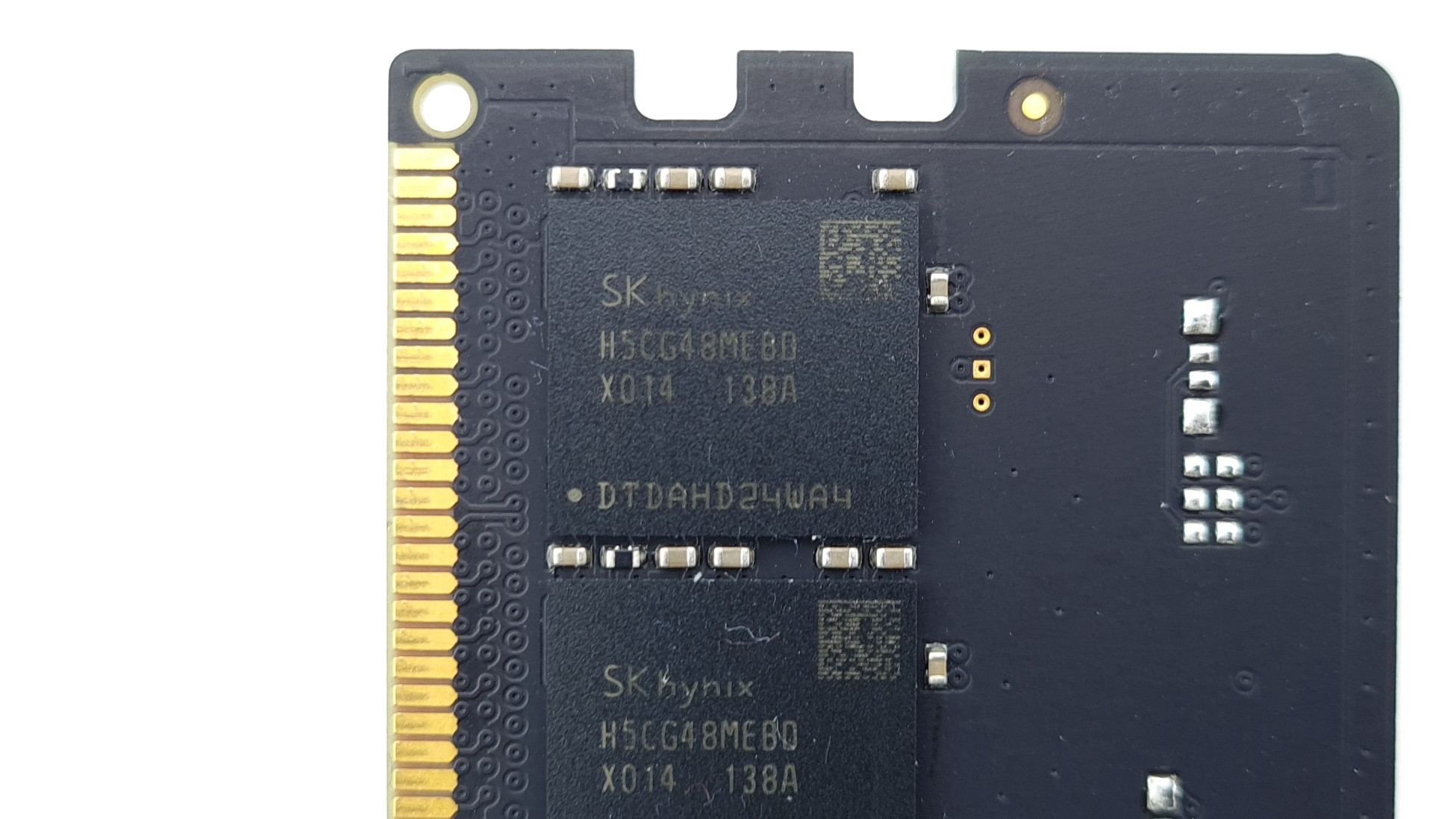
The memory ICs are chips from the manufacturer “SK hynix” with the product number “H5CG48MEBD”. According to the manufacturer’s public DRAM Component Decoder document, the memory devices thus have the following characteristics:
- H5C: Product type –DDR5
- G4: Memory density – 16 Gbit
- 8: Bit organization – x8
- M: generation – “first generation”, “M-The”
- EB: Binning speed – 4800 40-39-39
- D: Operating temperature – 0 – 95 °C
This results in the common name of the ICs as “DDR5 Hynix 16 Gbit M-Die” or in short form “5H16M”.
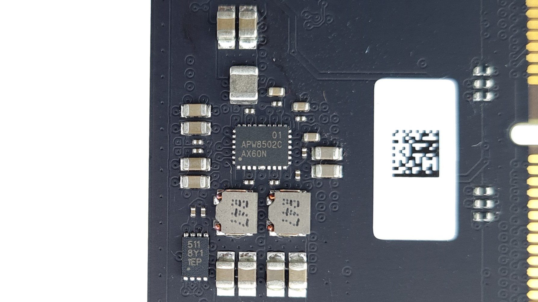
The PMIC (Power Management Integrated Circuit) is an “APW8502C” from Anpec, which is only recognized as a “JEDEC PMIC”, but can still supply voltages above the JEDEC limit of 1.435 V for VDD and VDDQ. The SPD-Eeprom is a package with the inscription “511 8Y1 EP” from Renesas, as we could already find out in the SPD.
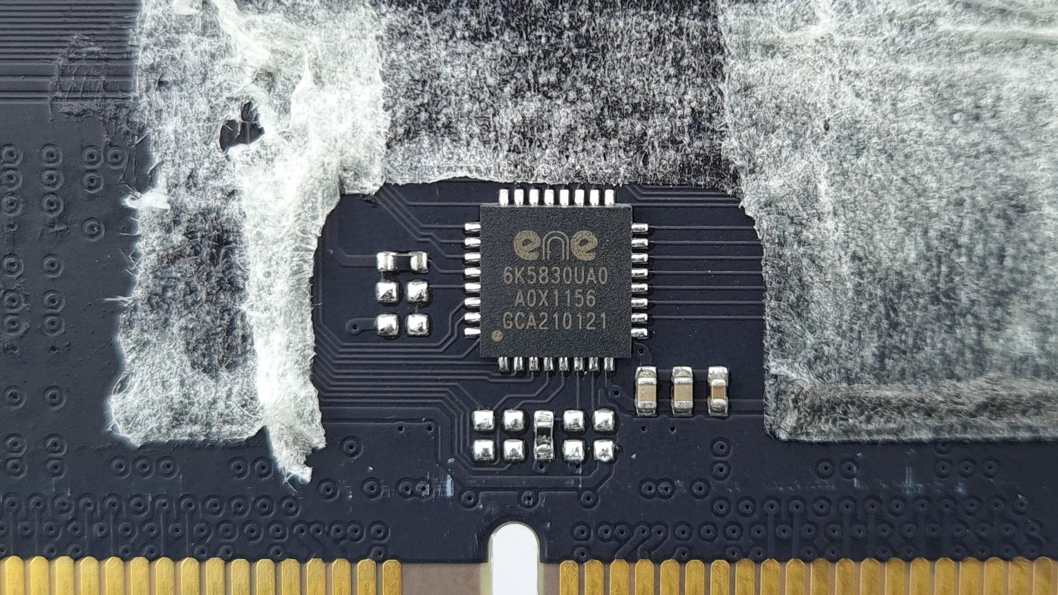
The RGB lighting is controlled by a “6K5830UA0” from ENE, which was already a well-known component on many DDR4 modules and thus ensures compatibility with various RGB software.
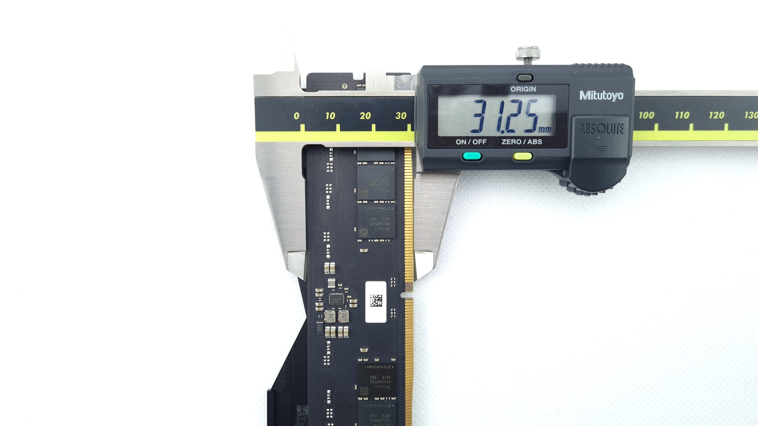
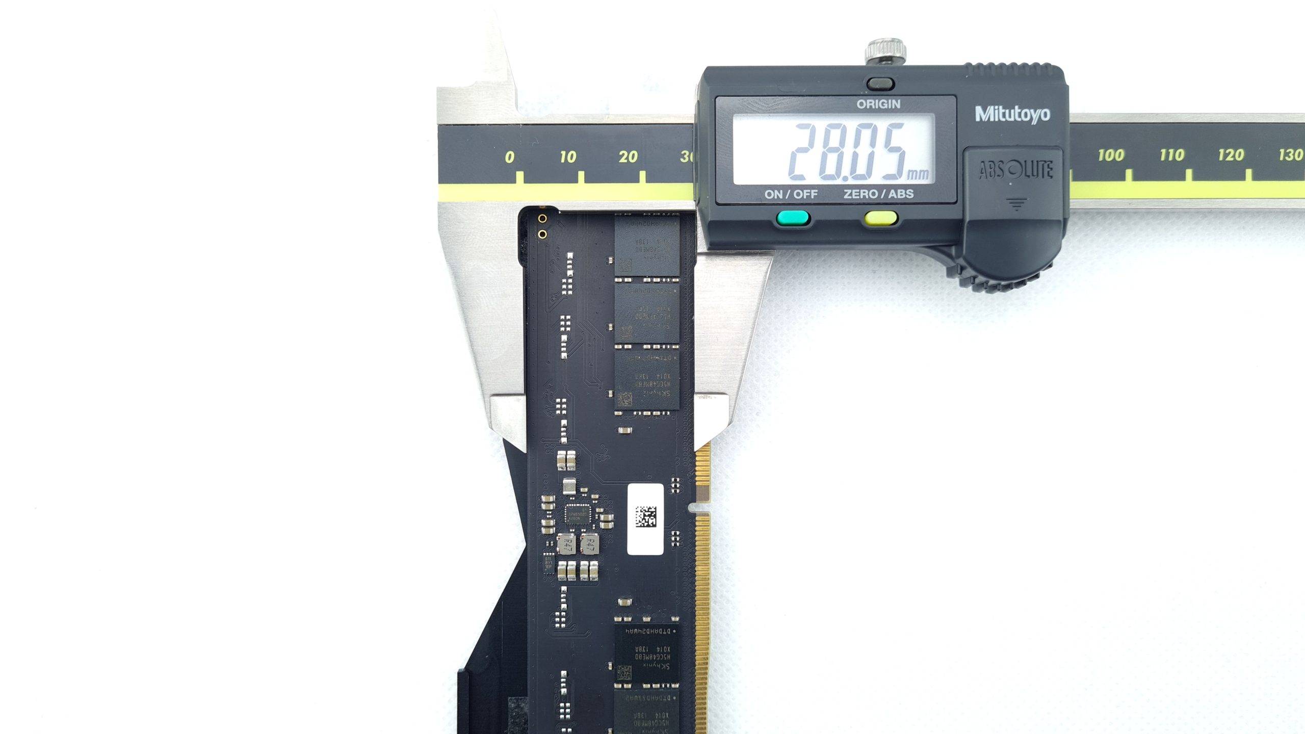
As typical for DDR5, the board has an 8-layer design, with 3 layers running on the outside and 2 in the center. For all those who want to install an aftermarket cooler like a water block, the following are also the dimensions of the sole PCB.
- 1 - Unboxing and design
- 2 - Dimensions and SPD information
- 3 - Teardown and PCB analysis
- 4 - Test systems and methodology
- 5 - Heatsink peformance and overclocking potential
- 6 - Synthetics – AIDA64, Geekbench 3, SPI32M, LinpackXtreme
- 7 - Gaming – SoTR, CS: GO, Cyberpunk 2077
- 8 - RGB lighting and conclusion


42 Antworten
Kommentar
Lade neue Kommentare
Urgestein
1
Mitglied
Urgestein
Urgestein
Veteran
Veteran
Urgestein
1
Urgestein
Urgestein
Urgestein
Mitglied
Mitglied
Mitglied
Mitglied
Mitglied
Mitglied
Mitglied
Alle Kommentare lesen unter igor´sLAB Community →