


The first impression of the modules is high-quality and the workmanship looks solid. ADATA has actually only applied what has already proven itself in DDR4, but why change a working formula? If you prefer a more extravagant design, ADATA XPG also offers the newly announced CASTER series.
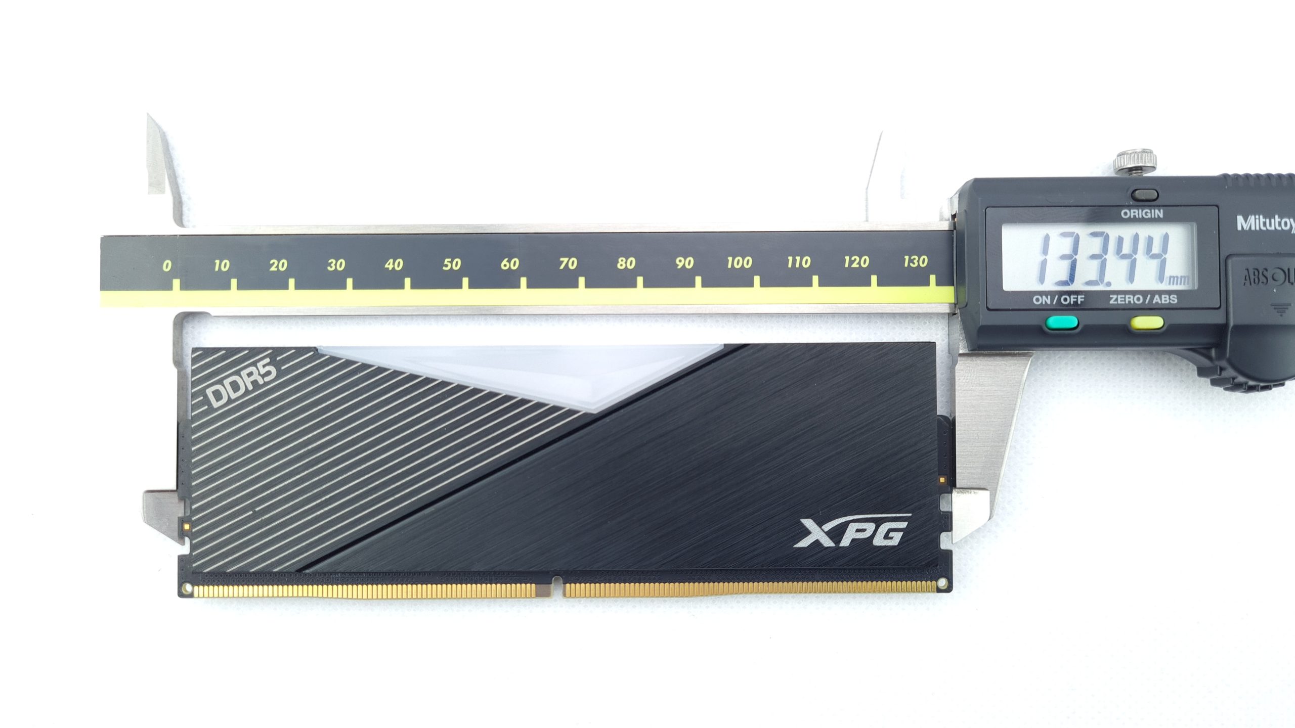
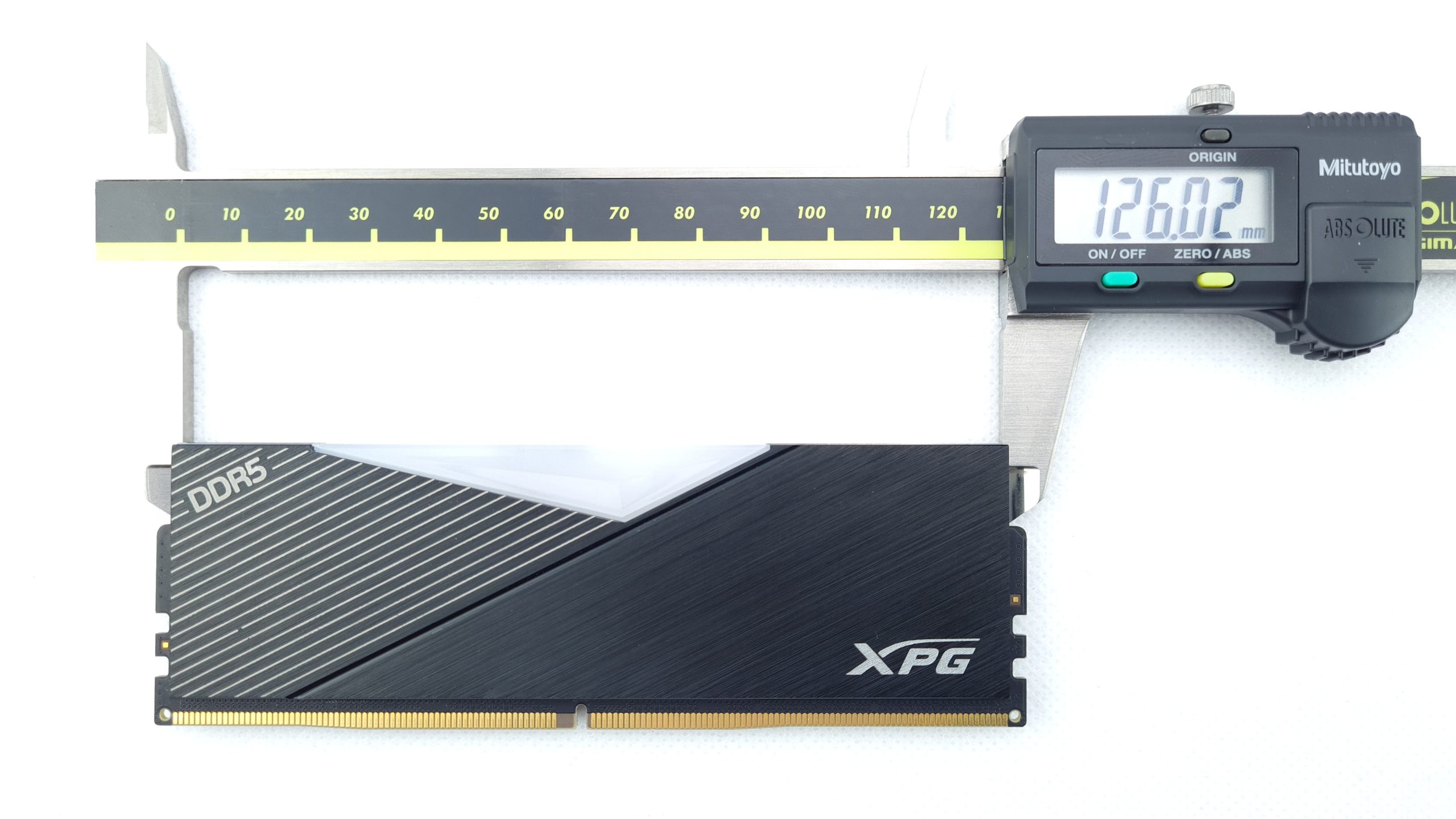
The modules measure the usual 133.5 mm for DDR5 in length, whereby only 126 mm are covered by the heat sink. This in turn means no overhang over the DIMM slot latches and thus easy handling of the modules during installation and removal.
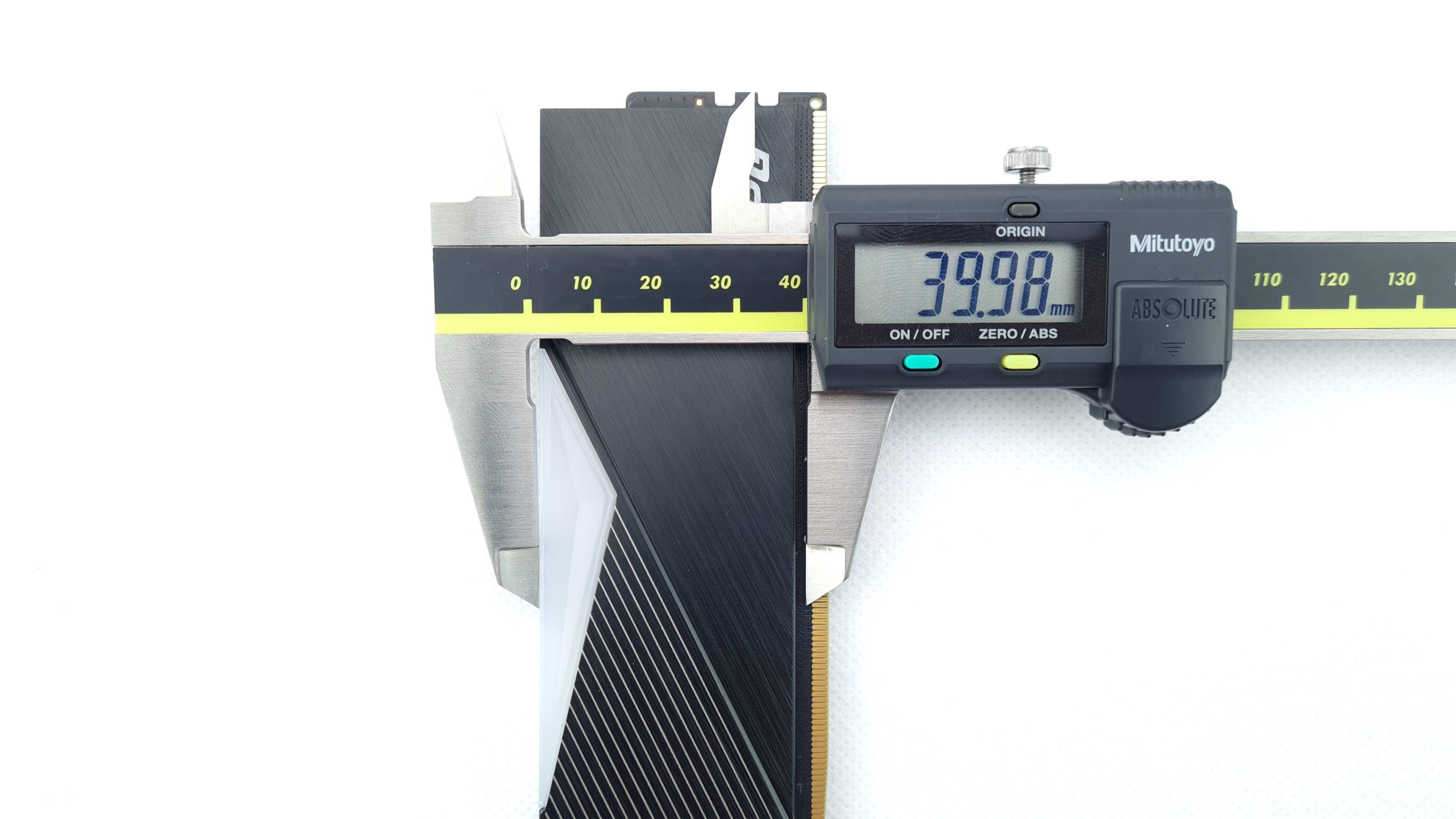
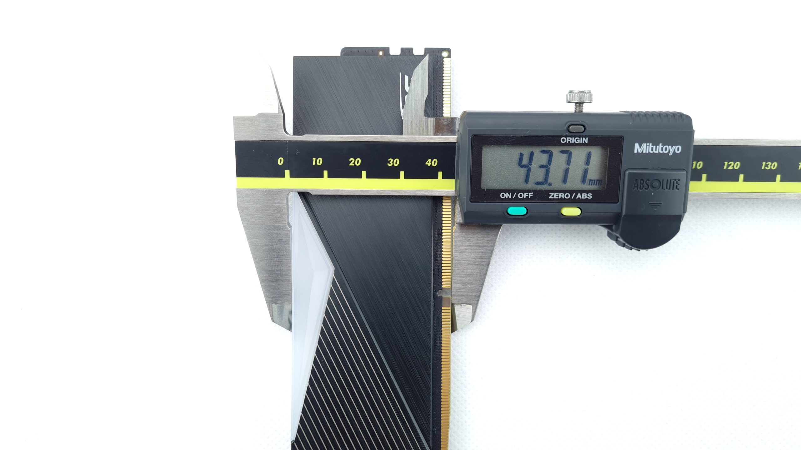
The modules reach just under 44 mm in height, 40 mm of which should be taken into account from the top edge of the DIMM slots for compatibility with any air coolers or radiators. A single module weighs 70 g, which also confirms the ambitions in the upper DDR5 midfield.
SPD information
To read out the SPD content, we again use the “Worktool” with its DDR5 SPD function from Asus on the Maximus Z690 motherboard.
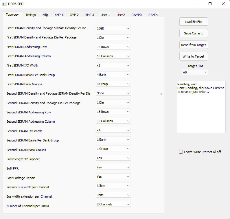
As usual with 16 GB DDR5 modules, we are talking about 16 Gbit memory chips with x8 connection and 8 bank groups with 4 banks each. These are in turn organized internally with 16 rows and 10 columns. Both 32 bit subchannels are identically equipped.
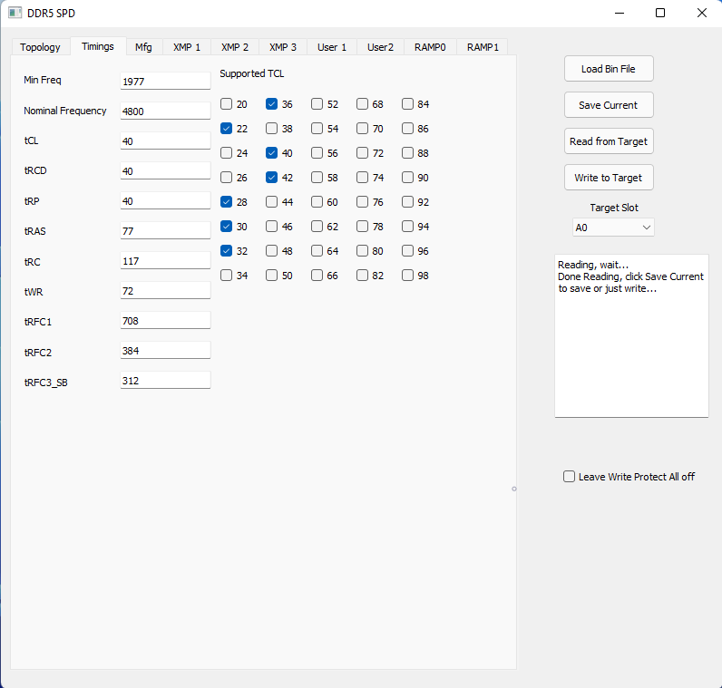
In the timings tab we find the clock rate specified by Hynix including timings according to the JEDEC standard for DDR4-4800 at 1.1 V VDD or VDDQ.
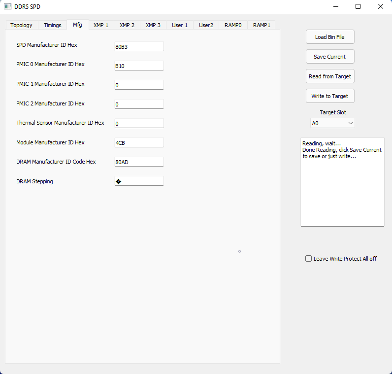
In the Mfg tab it gets more interesting, because here we find the Hex ID for the different module components. With the SPD, we were already able to identify “80B3” from the SPD manufacturer as Renesas in the last test (thanks again meilodasreh). We also already know the PMIC manufacturer ID with “B10” as Anpec. The DRAM manufacturer code “80AD” should therefore stand for SK Hynix and only the module manufacturer with “4CB” is still a mystery to me. If you have any ideas here, feel free to let me know in the forum. The DRAM stepping is output here as a non-decodable character, but as we will see later, it is “1st gen” or “M-Die”.
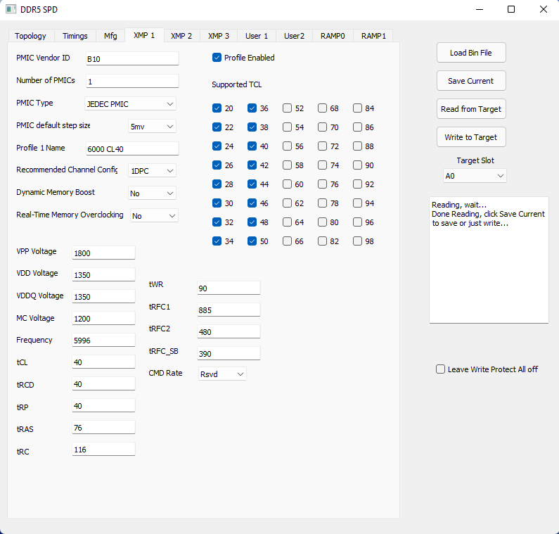
The full XMP profile for DDR5-6000 is 5996 Mbps with timings tCL 40, tRCD 40, tRP 40, tRAS 76, tRC 116, tWR 90, tRFC1 885, tRFC2 480, and tRFC_SB 390, at 1800 mV VPP, 1350 mV VDD, 1350 mV VDDQ, and 1200 mV VDD2. Asus only calls the latter differently on their boards as “MC Voltage”. Dynamic Memory Boost and Real-Time Memory Overclocking are not supported and the recommended configuration is limited to one DIMM per channel. With such high clock rates, combining multiple kits, albeit with the same specification, is therefore not advisable if you expect plug and play.

- 1 - Unboxing and design
- 2 - Dimensions and SPD information
- 3 - Teardown and PCB analysis
- 4 - Test systems and methodology
- 5 - Heatsink peformance and overclocking potential
- 6 - Synthetics – AIDA64, Geekbench 3, SPI32M, LinpackXtreme
- 7 - Gaming – SoTR, CS: GO, Cyberpunk 2077
- 8 - RGB lighting and conclusion


42 Antworten
Kommentar
Lade neue Kommentare
Urgestein
1
Mitglied
Urgestein
Urgestein
Veteran
Veteran
Urgestein
1
Urgestein
Urgestein
Urgestein
Mitglied
Mitglied
Mitglied
Mitglied
Mitglied
Mitglied
Mitglied
Alle Kommentare lesen unter igor´sLAB Community →