


As is often the case, my tool of choice for RAM module disassembly is a standard household hair dryer. After a short warm-up, the two halves of the cooler can be slowly levered off the PCB with relatively little resistance. For this I use a plastic spatula and work my way along the bottom edge of the modules, starting with the side with the memory chips.
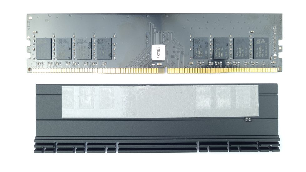
Here you can see again clearly how actually just 6 of the 8 memory chips have contact with the thermal pad. Of course, we don’t know why Kingston saves at this point or doesn’t simply split the pad in two and move the halves to the outside. Cooling performance is still more than adequate, at least for XMP operation, but users with serious OC ambitions would probably want to perform an upgrade here themselves.
The foam tape on the back of the PCB is, as is often the case, a bit stubborn and weaker than the glue that holds it to the PCB and cooler. So a little more sensitivity is needed here if you want to reuse this. But here, too, the time required is kept within limits at just a few minutes, so that the heat sink design as a whole can shine with proper maintainability.
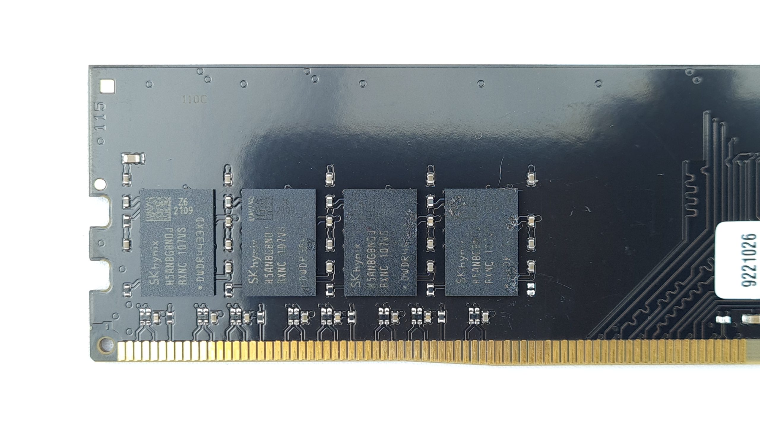
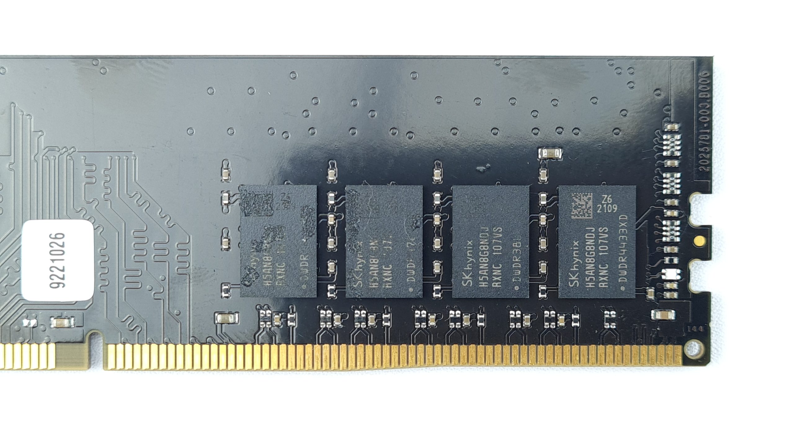
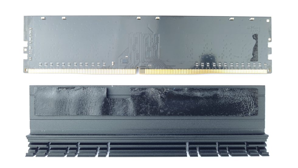
Shiny is a good keyword, because the PCB reflects light a lot more than I’ve seen from other RAM modules. In addition, the PCB is relatively flexible, which could indicate specificities in the production process. To the naked eye, the layout is relatively close to the A2 reference design with the two sets of 4 memory chips as far out as possible and close to the contact fingers.
These are as you would expect from such high clock speed DDR4 8 Gbit DJR, recognizable by the label “SK hynix H5AN8G8NDJRXNC 107VS”. Next to it, you’ll also find a QR code, an inscription “Z6 2109” which could stand for the date of manufacture, and another coding that differs from chip to chip, presumably a binning label.
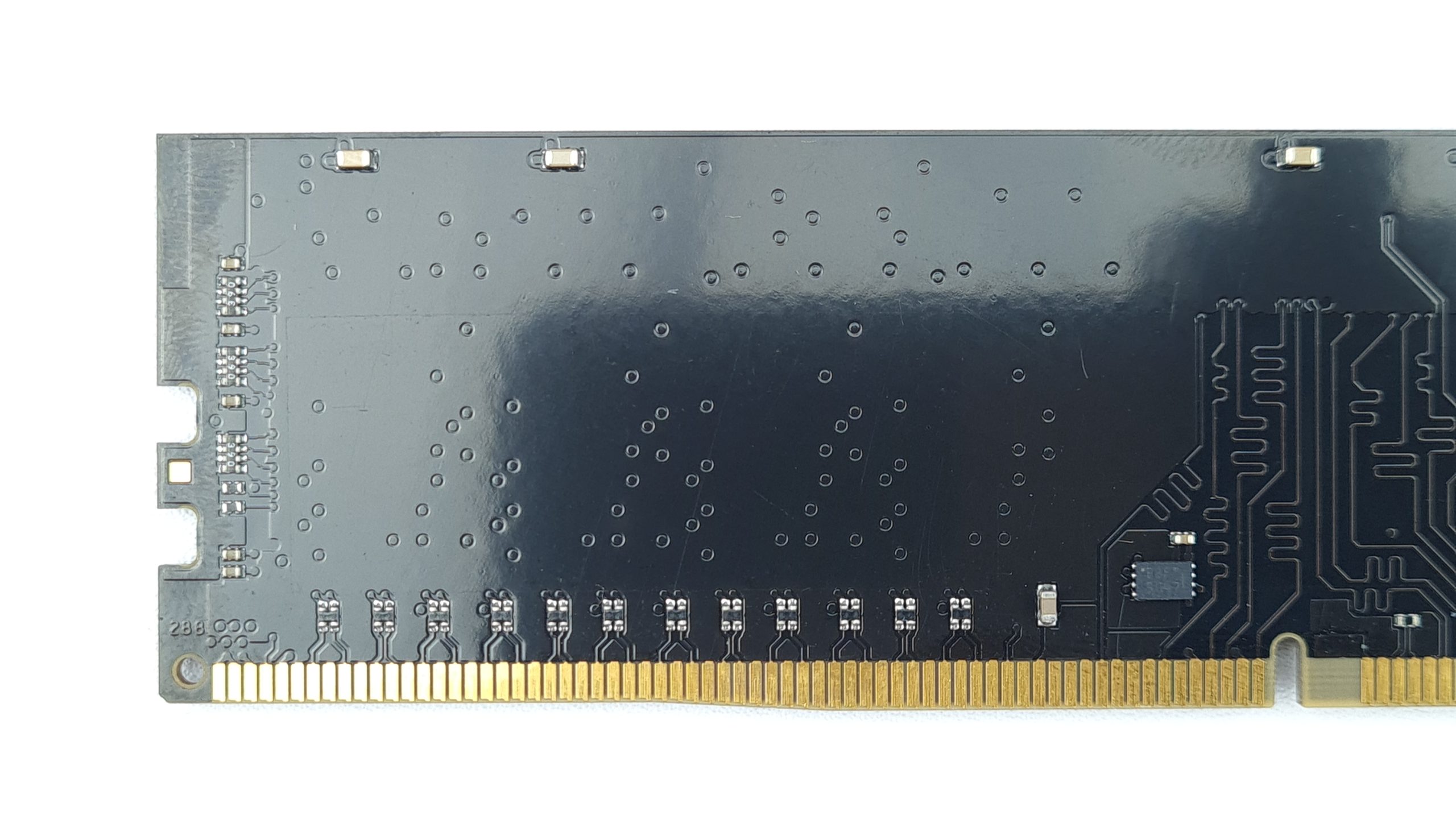
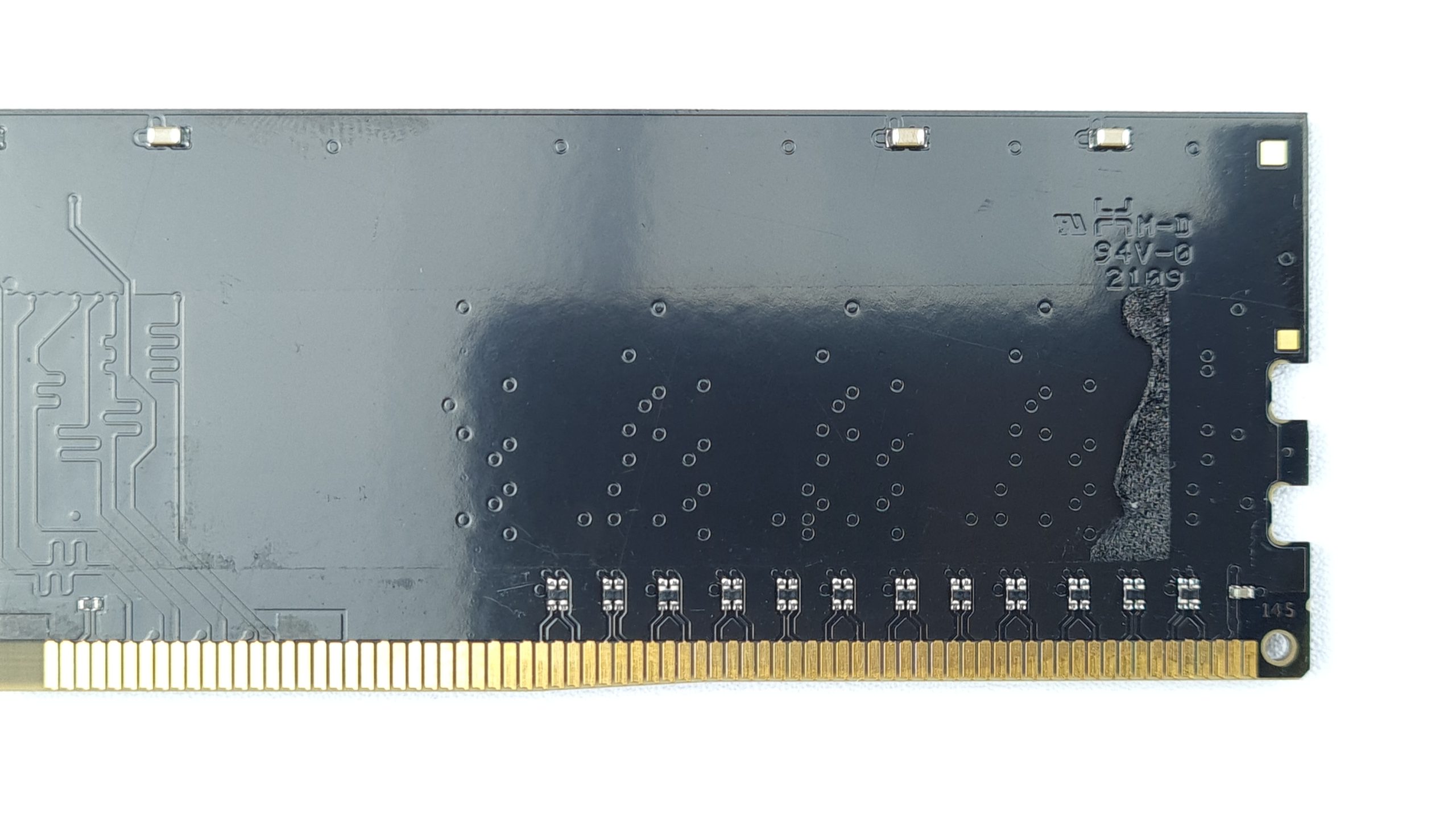
The back, on the other hand, looks pretty unspectacular. Besides the SPD EEPROM package labeled “88FT 8047” there are only a few MLCC capacitors along the edges of the module. Judging from the logo in the embossed top right, Tripod Tech should be the OEM, at least for the circuit board (thanks again to Mick for the tip!).

- 1 - Introduction and SKUs
- 2 - Packaging and looks
- 3 - SPD and heatsink performance
- 4 - Teardown and PCB analysis
- 5 - Test systems and methodology
- 6 - XMP compatibility and overclocking
- 7 - Synthetic benchmarks – AIDA64 and Geekbench 3
- 8 - Gaming – Cyberpunk 2077 in UHD, QHD, FHD
- 9 - Final thoughts and conclusion


8 Antworten
Kommentar
Lade neue Kommentare
Urgestein
Urgestein
Veteran
Veteran
Veteran
Mitglied
Moderator
Urgestein
Alle Kommentare lesen unter igor´sLAB Community →