


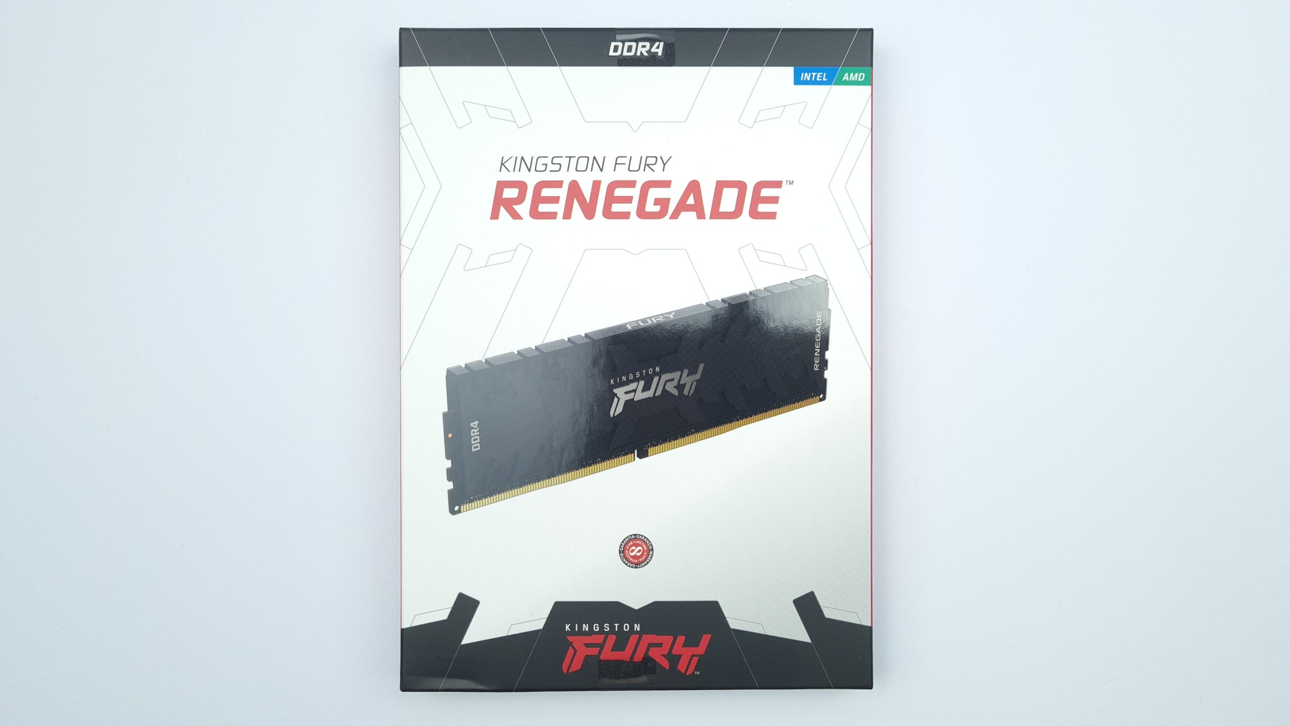
But before we get to the oh so important inner values, first a few impressions and words about the exterior. The packaging makes a fresh and high-quality impression. Besides a picture and product name of the modules, the compatibility with Intel and AMD platforms and the “Limited Lifetime Warranty” are advertised.
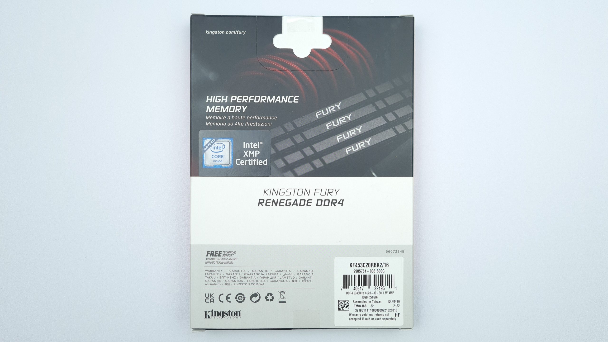
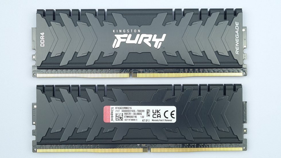
On the back, there’s another reference to XMP certification for Intel, which, noted in advance, might become a bit more of a gray area at 5333 Mbps than it already is, but more on that later. Furthermore we find here the SKU number of the kit KF453C20RBK2/16, the XMP profile specified with DDR4 5333 MHz CL20-30-30 1.6V and the capacity with 16GB (2x8GB). It’s also interesting that Kingston doesn’t even list the tRAS timing from the XMP profile here.
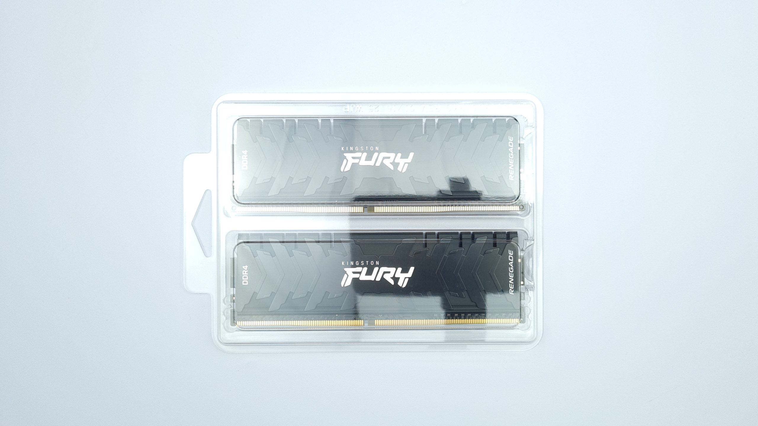
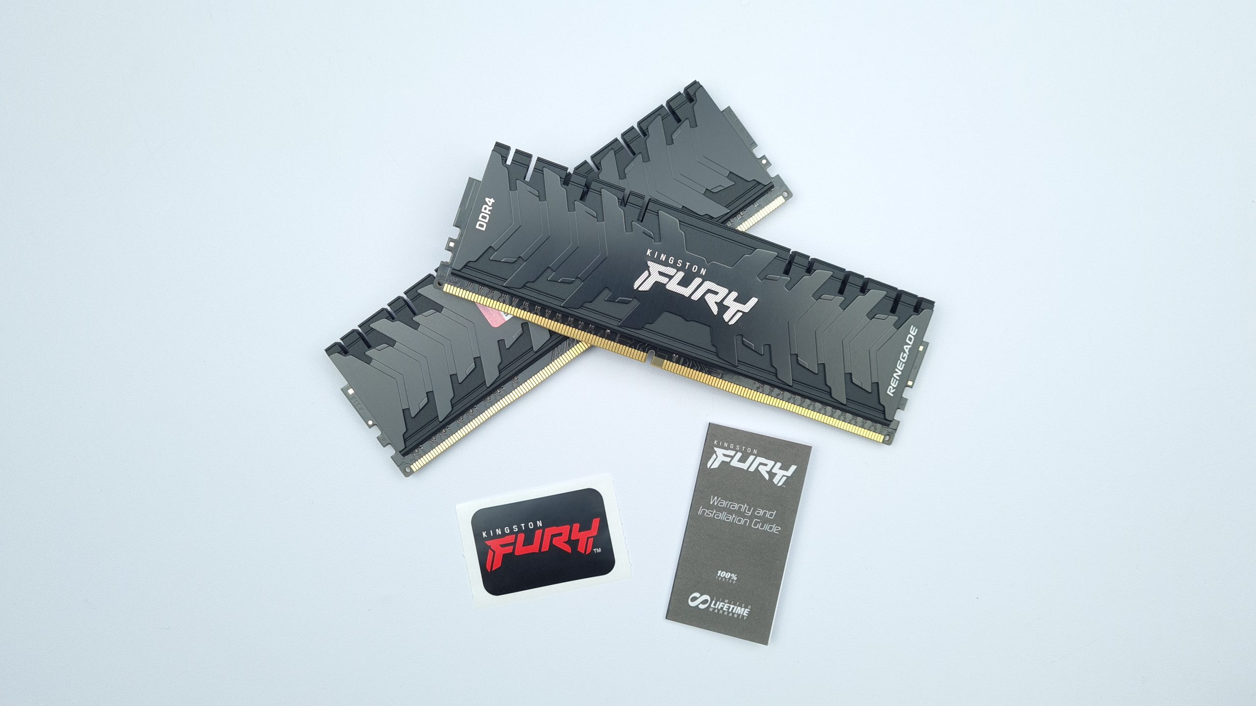
Inside you will find the modules in a transparent plastic carrier, a Warranty and Installation Guide and a Kingston Fury sticker. Due to their weight and the massive heat sink, the modules appear solid and high-quality at first glance. The heatsink halves are each made of two parts, consisting of a black anodized main part and a black painted accent element glued on top of it, which reminds a bit of a mirrored fishbone and looks brighter or darker than the main part depending on the light reflection.
On one side is the sticker with the product, serial number, operating voltage and some other information, and on the other side is the silver reflective “Kingston Fury TM” logo with vertical white “DDR4” and “RENEGADE” lettering on the ends of the heatsink. In addition to the dimensions of 133.35 x 42.2 x 8.3 mm already described in the data sheet, the weight of 69 g per module should also be mentioned.
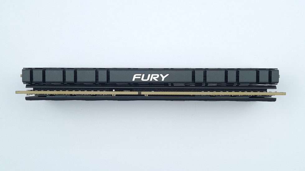
From above you can see the several layers of the heatsink. On the anodized inner part once again there is a white “Fury” lettering printed in the middle. Along the top, the element also has vertical cuts each in pairs, which should be beneficial both visually and for cooling performance.
From below we can already see that these are single-sided modules. While on one side you can see the 8 memory chips, on the other side there is only a foam placeholder between the board and the heatsink. The memory chips, in turn, are thermally connected to the heat sink with a thermal pad, at least partially. Unfortunately, one chip has very little contact area and the one on the far right has none at all.
All memory chips, even DJR, become unstable above a certain temperature and even if you stay far away from the JEDEC-specified 85° C, it’s a pity for an overclocking-focused product like this that the saving of 15 mm thermal pad could possibly lead to instability at the limit.
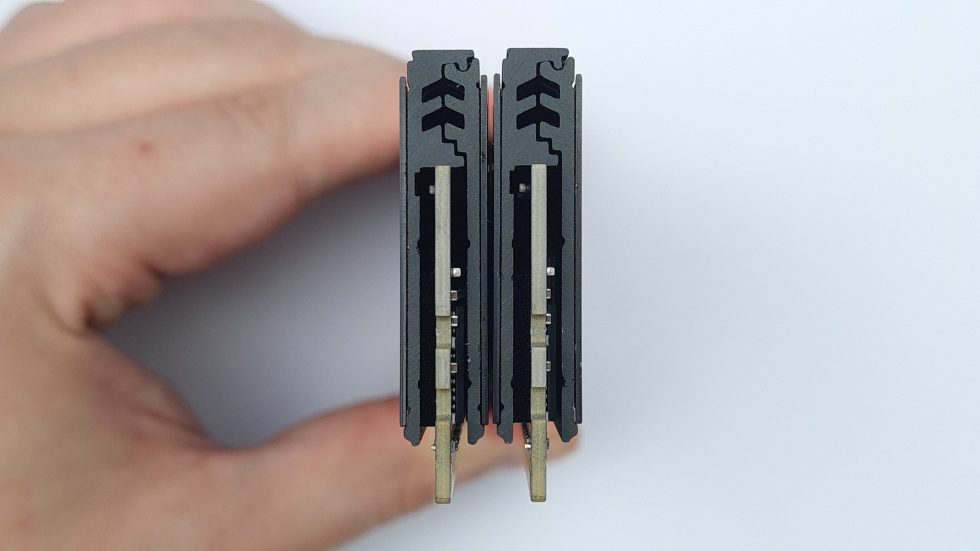
From the side, the construction of the two heatspreader halves can be easily seen, with one hooking into the other above the PCB and thus requiring no further attachment there. So the only attachment points are the two adhesive surfaces along the PCB and memory chips respectively, which should make for easy disassembly, but more on that in a moment.

- 1 - Introduction and SKUs
- 2 - Packaging and looks
- 3 - SPD and heatsink performance
- 4 - Teardown and PCB analysis
- 5 - Test systems and methodology
- 6 - XMP compatibility and overclocking
- 7 - Synthetic benchmarks – AIDA64 and Geekbench 3
- 8 - Gaming – Cyberpunk 2077 in UHD, QHD, FHD
- 9 - Final thoughts and conclusion


8 Antworten
Kommentar
Lade neue Kommentare
Urgestein
Urgestein
Veteran
Veteran
Veteran
Mitglied
Moderator
Urgestein
Alle Kommentare lesen unter igor´sLAB Community →