


Since there is currently no DDR5 compatible version of the Thyphoon Burner, the software I liked to use with DDR4 to read the SPD, we have to help ourselves differently today. Fortunately there is the “Worktool” or “Tool.exe” for the Asus Maximus boards, with which various components of the Z690 platform can be monitored and controlled from the OS, like also the SPD of DDR5. The presentation is a bit spartan or cryptic, but we can still gain the most important information this way.
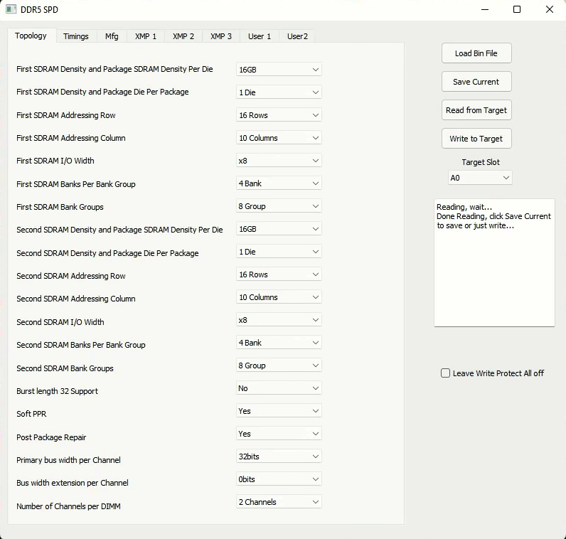
In the Topology tab we find basic information about the organization of the memory devices. The capacity is stated here with 16 GB, whereby 16 Gb should mean gigabit. Each of the dies has 16 rows and 10 columns into which the memory addresses are divided. The bit organization of the IO is again specified as x8, resulting in 4 dies per subchannel, or 8 dies per channel. Since the modules have a total of 8 dies each, they are single-rank modules. Each die or IC contains 8 bank groups of 4 banks each, confirming my previous assumption of 32 banks total. The information is split between “First SDRAM” and “Second DRAM” sections, which could indicate that the subchannels could theoretically be populated differently in DDR5. Further down we find the information about the two 32-bit wide subchannels.
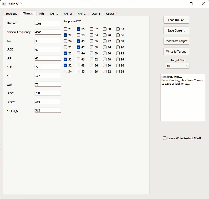
In the timings tab, as usual, we only find the specifications according to JEDEC as originally designed by Samsung for these memory chips. The nominal clock speed of DDR5-4800 is given here with timings tCL 40, tRCD 40, tRP 40, tRAS 77, tRC 117, tWR 72, tRFC1 708, tRFC 384, tRFC3_SB 312. Although additional supported and thus implicitly unsupported values are given for tCL, in my experience this does not seem to matter in reality. For example, tCL 34 also works without any problems. At this point it is important to mention again that DDR5 officially supports only even values for the tCL.
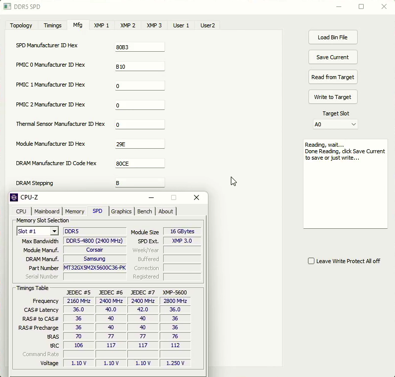
In the Mfg tab we find the manufacturers of the various module components as identification numbers in hex code. B10 should therefore stand for ANPEC, 29E for Corsair and 80CE for Samsung. The ID 80B3 of the SPD manufacturer points to Renesas which would also clear up that secret (Thanks meilodasreh! 😉 ). Again, DRAM Stepping lists revision B, which could stand for the already identified “B-Die” ICs.
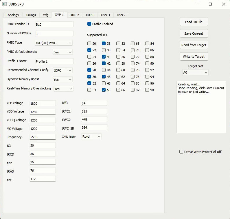
In the XMP 1 section we now find the complete XMP profile and some interesting info about the PMIC. There is 1 PMIC of the type “XMP (OC) PMIC” installed, which indicates on the one hand that DDR5 modules could also have several PMICs, e.g. for dual-sided layouts, and on the other hand that the voltages VDD and VDDQ can be raised above the 1.435 V limited by JEDEC with this PMIC. Furthermore we find the info that the recommended module configuration for this profile is “1DPC”, that means 1 DIMM module per channel. So running 2 identical DDR5 XMP kits on a 4-DIMM motherboard in dual-rank is not recommended and does not work without further manual settings according to my tests. Dynamic Memory Boost and Real-Time Memory Overclocking are also supported.
The full XMP 3.0 profile is also specified with the following voltages: 1800 mV VPP, 1250 mV VDD, 1250 mV VDDQ and 1200 mV MC Voltage. By the way, the latter is only loaded in the Asus BIOS if the “XMP II” option is selected. However, this also assumes that the value has been programmed into the SPD by the RAM manufacturer, which Corsair has done in exemplary fashion. The effective frequency is specified as 5593 MT/s with timings tCL 36, tRCD 36, tRP 36, tRAS 76, tRC 112, tWR 84, tRFC 825, tRFC2 448, tRFC_SB 364 and CMD Rate Rsvd, the latter of which should stand for the platform standard 2T.
Heatsink test
Of course a test of the heatsinks may not be missing again, because this has not become a less important topic with DDR5. And also because the manufacturers of the currently available DDR5 memory chips do not integrate temperature sensors on the package, the measurement of the “SPD Hub Temperature”, as it can be read out in HWinfo, is not necessarily indicative for cool and thus stable running memory chips further down on the board, as Igor had already shown.
In our test, as always, the TestMem5 v0.12 software with the profile “Extreme1@Anta777” is used due to its high and constant thermal load. For measurement, a type K temperature sensor was placed centrally on the warmer module at the level of the memory ICs, between the circuit board and the heatsink. In an interval of 500 ms the delta to the room temperature is formed and the course is plotted until the maximum value has been reached in the test run.
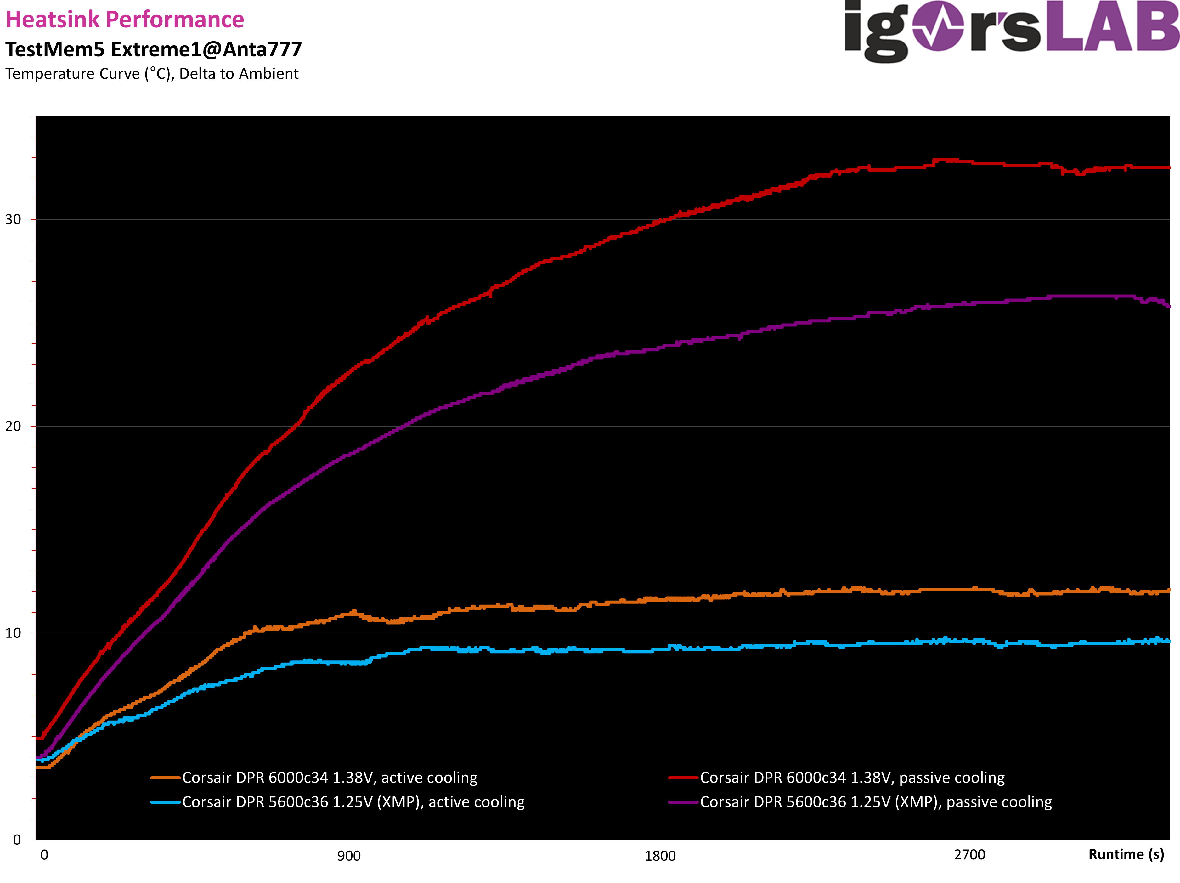
The modules were tested in the XMP profile with 1.25 V VDD and VDDQ voltage and in the overclocked state with 1.38 V each (details later). In addition, the configurations were each tested with passive and active cooling. The latter is implemented with a 120 mm fan that rests directly on the modules and blows air downwards towards the DIMM slots. Since the Asus Maximus Z690 Apex motherboard has two DIMM slots, the modules are right next to each other without a slot gap as would occur on 4-DIMM motherboards, which also makes the task for the heatsinks more difficult. Two test runs were made in each case and the one with the higher maximum temperature was kept.
The most important thing first, all configurations, even the passively cooled ones survive the TM5 without errors. So the cooler of the Corsair Dominator Platinum RGB modules does a good job. The difference between passive and active cooling as well as the difference in voltage is clearly noticeable in the test and without active cooling you should probably not exceed the 1.4 V limit – that much I can say in advance. I’ll leave the results as they are, because we also lack the reference to other DDR5 kits with similar voltages and clock rates. But one thing is for sure, even though DDR5 has become supposedly more efficient with the same power consumption, the waste heat is still not negligible.

- 1 - Introduction and unboxing
- 2 - Design and lighting
- 3 - Dimensions, teardown and PCB analysis
- 4 - SPD infos and heatsink performance
- 5 - Test systems and methodology
- 6 - XMP compatibility and overclocking
- 7 - Synthetic benchmarks – AIDA64, GB3, LinpackXtreme, SPI 32M
- 8 - Gaming 1440p – Cyberpunk 2077, SoTR, CSGO
- 9 - Gaming 1080p – Cyberpunk 2077, SoTR, CSGO
- 10 - Summary and conclusion


8 Antworten
Kommentar
Lade neue Kommentare
Urgestein
Mitglied
Urgestein
Urgestein
Veteran
Urgestein
Mitglied
Mitglied
Alle Kommentare lesen unter igor´sLAB Community →