


Teardown
To remove the cooler from the board, only the adhesive needs to be briefly heated with a hairdryer. The two halves of the cooler can then be carefully levered off. The IC side reveals the adhesive thermal pads, which are the same height for memory devices and PMIC. At the top of the cooler, or here at the very bottom of the picture, a reflective foil is added, which should help the uniformity of the lighting.
wonderplugin_gallery id=5404]
On the back, the design is effectively identical, except that ICs and PMIC are replaced with foam placeholders, and instead only the components for controlling the RGB lighting are found on the PCB.
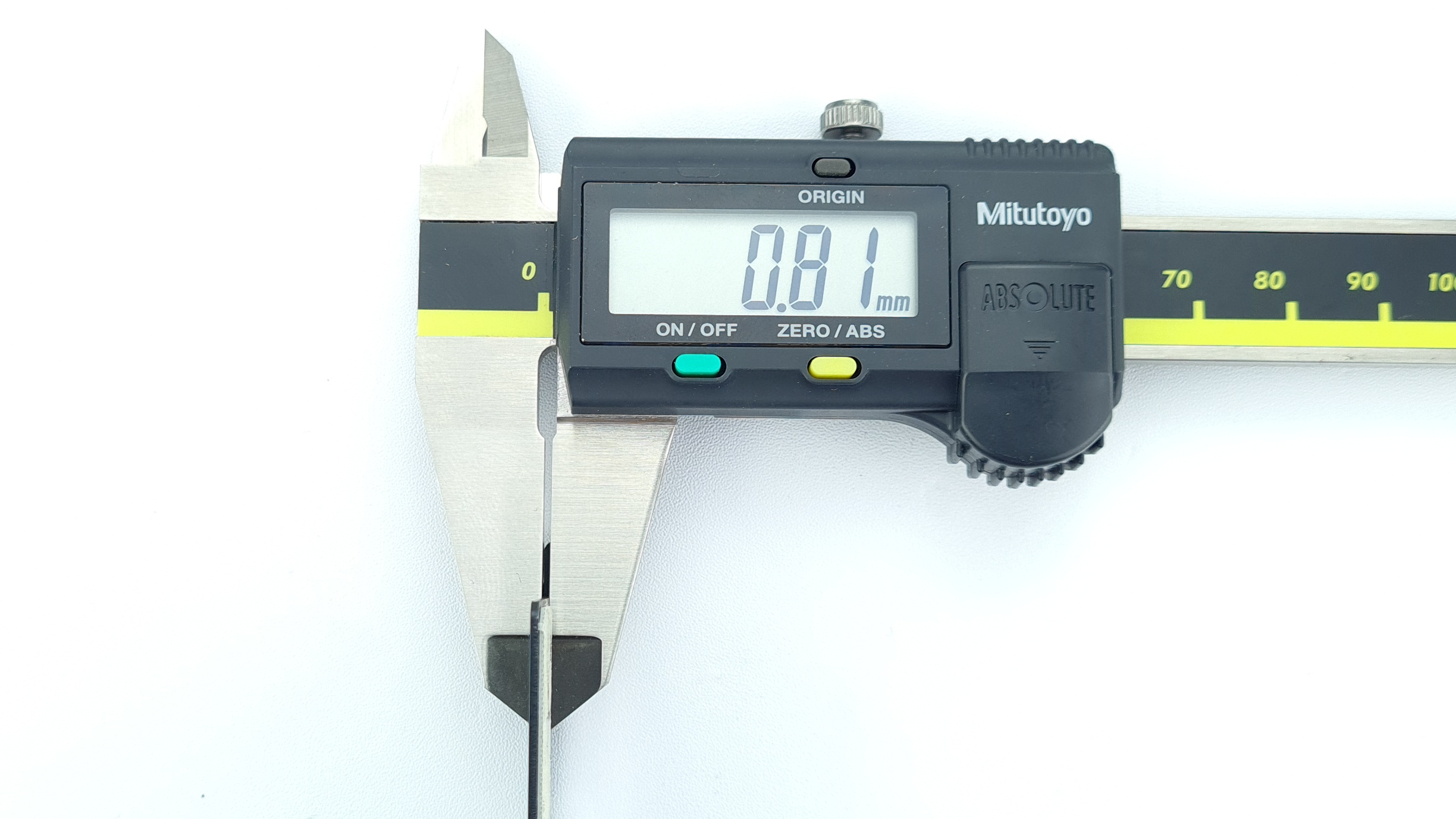
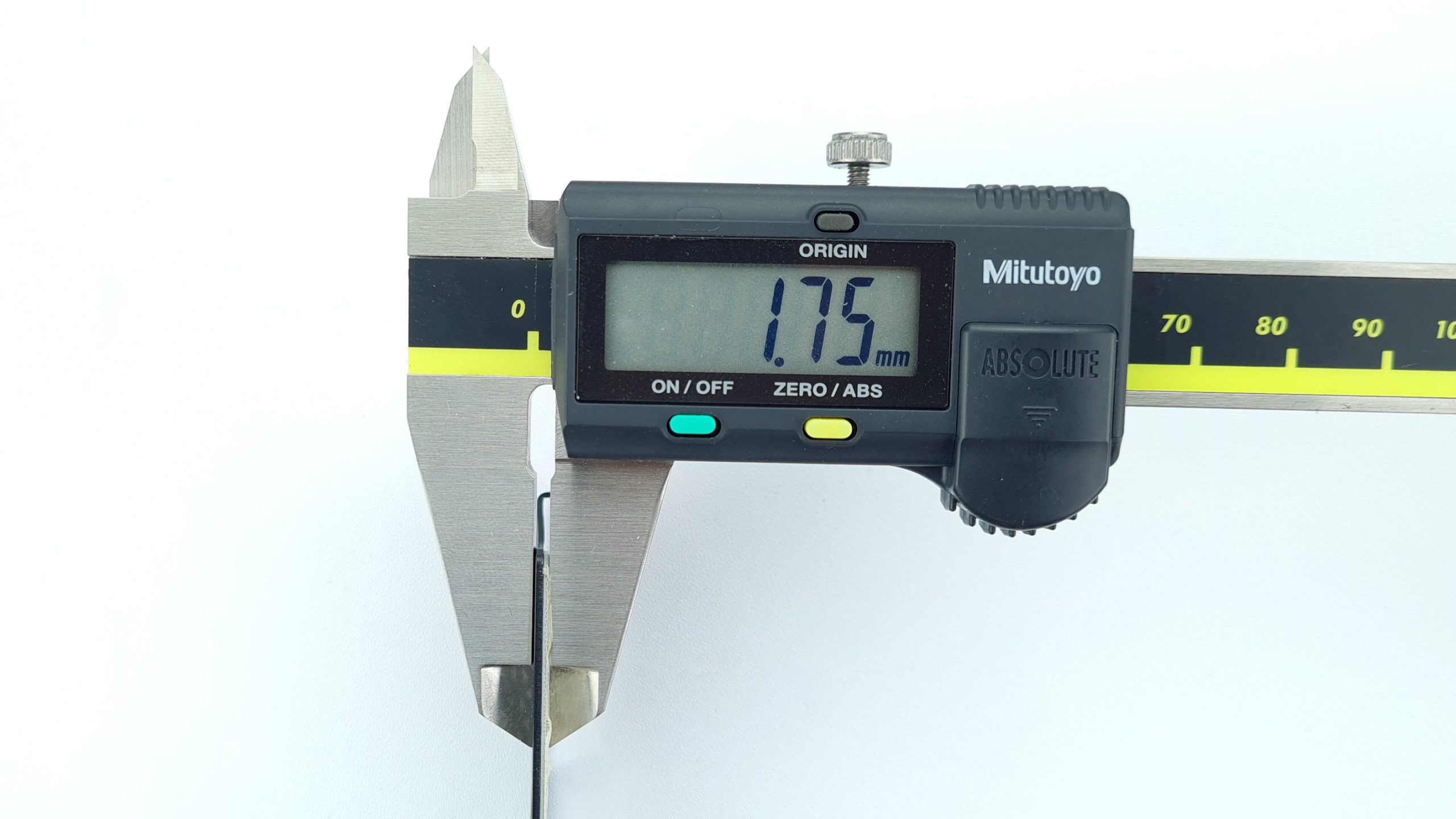
The cooler halves are made of anodized aluminum with a thickness of approx. 0.8 mm, on which the 1 mm thick thermal pads are in turn mounted. This cooler design is not lavish, but as we saw in the heat test, it works sufficiently well for XMP operation. And since the JEDEC PMIC doesn’t provide more than 1.435 V of voltage anyway, there is just enough cooling for overclocking. That’s a good fit, at least for this SKU.
PCB analysis
Now let’s move on to the analysis of the board itself. You can see directly from the label on the top right that the OEM is Brain Power from Taipei, Taiwan. In addition to the type designation “BP 4M-1 E186014”, there is also the “94V-0” designation and the UL logo in accordance with safety certifications for the North American market.
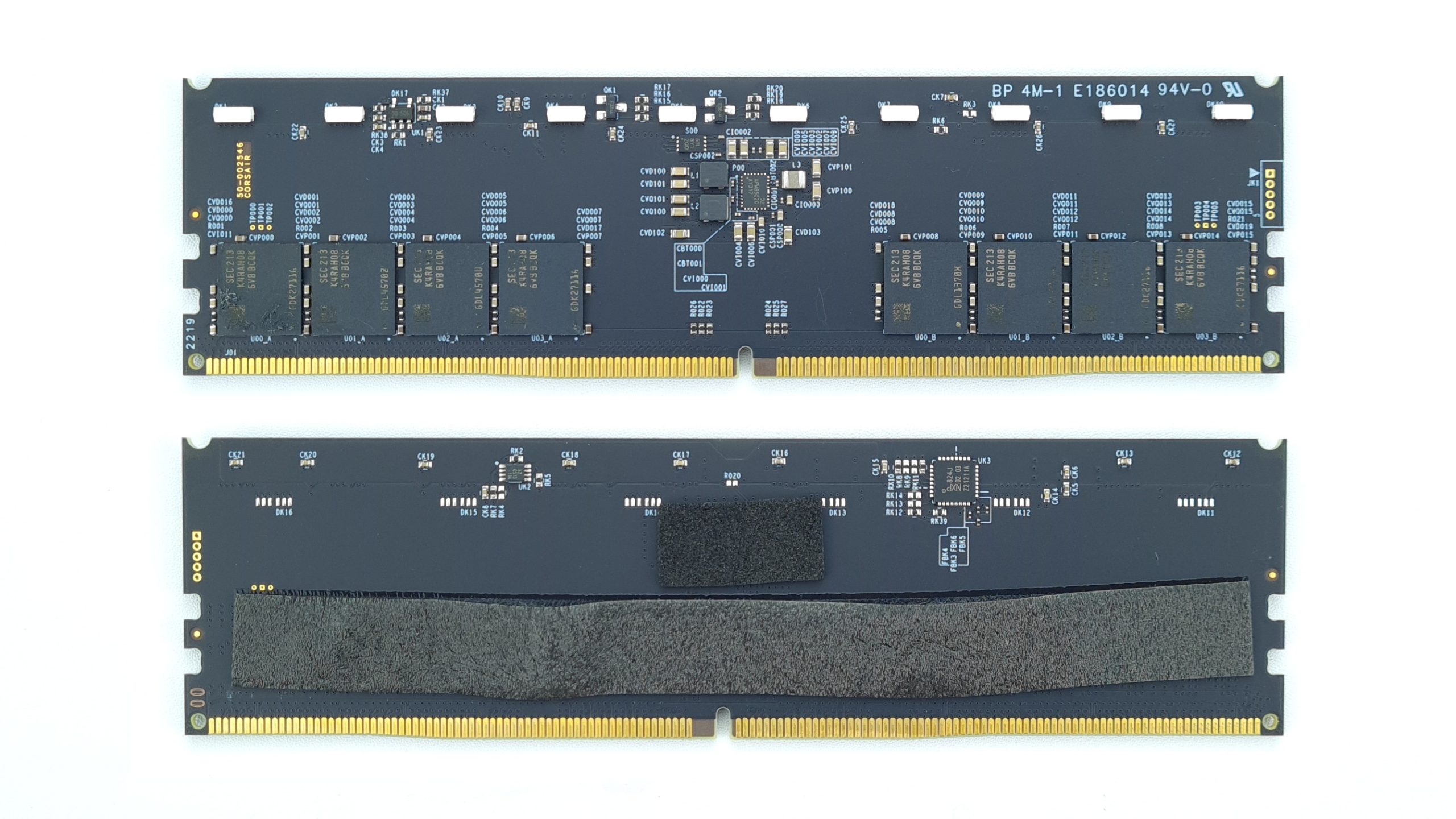
The actual design revision of the DDR5 module should be found on the top left with the vertical gold imprint. “50-002546 CORSAIR” suggests that Corsair conceptualized the board layout and Brain Power manufactures them under contract. The inscription “2219” at the bottom left probably hides the date of manufacture as calendar week 19 of this year.
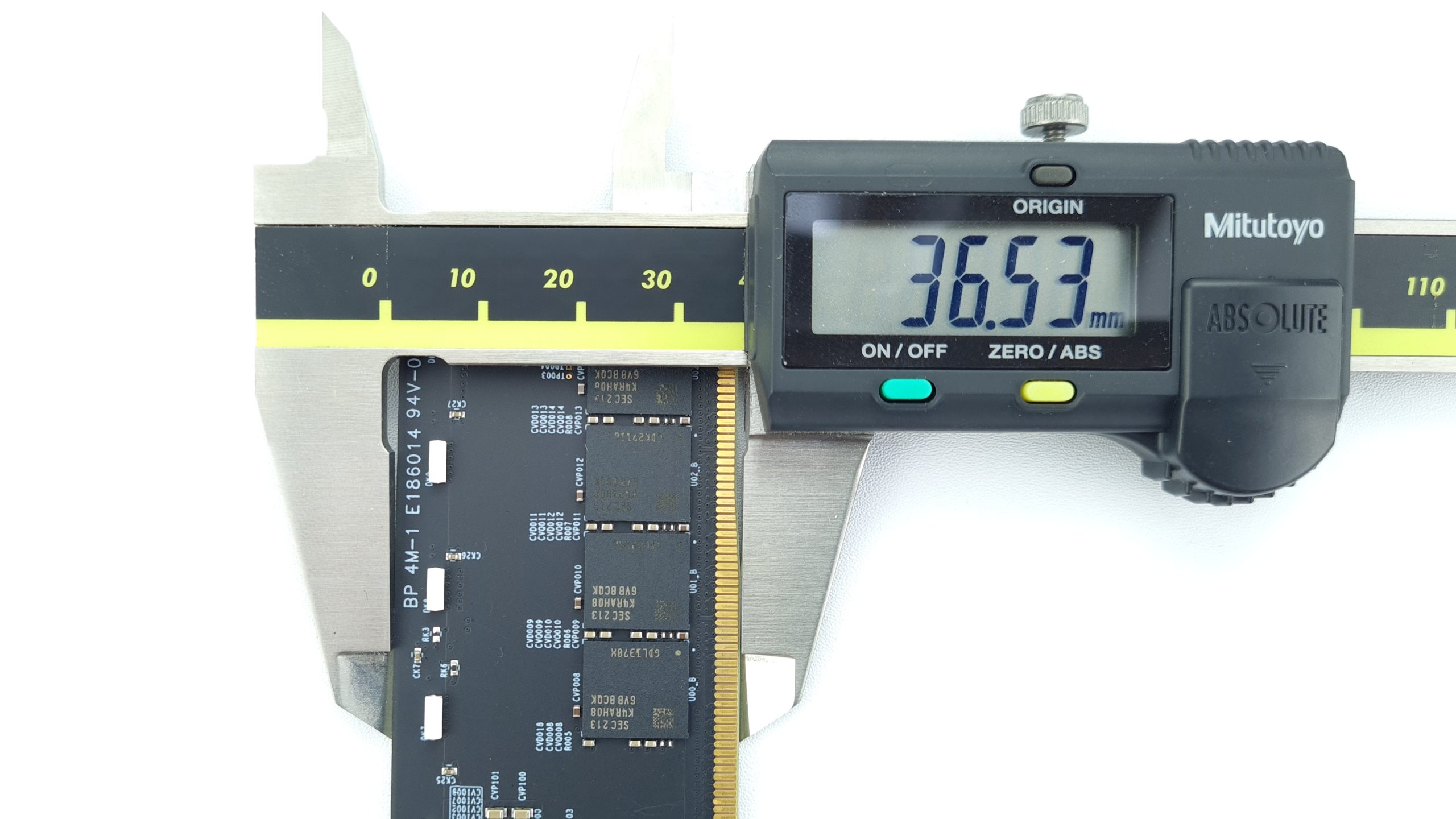
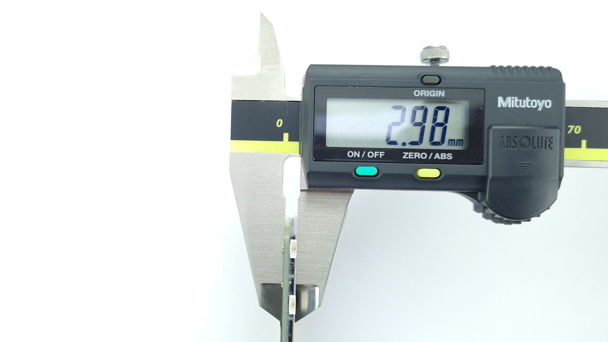
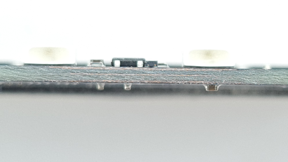
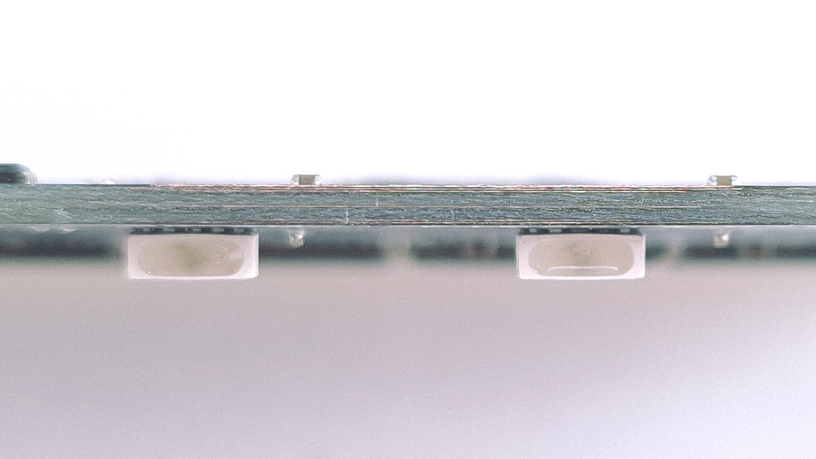
The PCB is a bit taller than the JEDEC A0 reference design at about 36 mm, and for that reason alone it is probably difficult to use for aftermarket coolers. In addition, the tallest components on the board are actually the RGB LEDs, which brings the board’s thickness to a maximum of 3 mm. ICs and PMICs are much lower, so the Vengeance RGB modules should be rather uninteresting for cooler conversions.
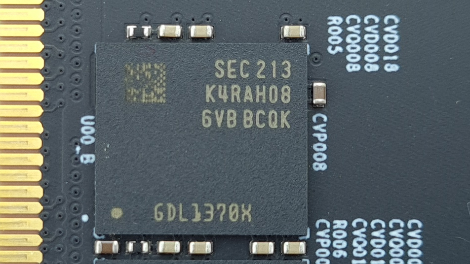
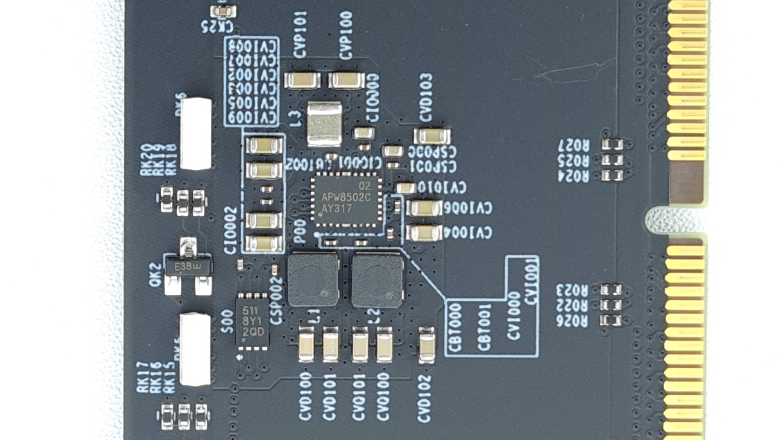
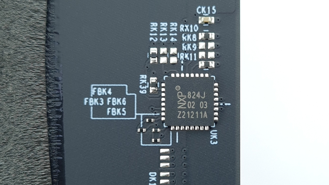
ICs are Samsung 16 Gbit B-Die DDR5 memory chips as already identified in the SPD. Unlike DDR4, the DDR5 B-Dies are not absolute high-end components and are about midfield in terms of clock potential and performance, at least at the time of this review. PMIC is an APW8502C from Anpec and RGB control is provided by an NXP 824J as in other Corsair DDR5 modules.
The number of layers on the board presented me with a challenge in this case. Because no matter where I uncovered the layers, all the copper layers really didn’t show up, or they weren’t laid out symmetrically with a single layer in the middle and different numbers on the sides, which doesn’t really make sense from a production standpoint. Instead, it’s probably an 8-layer design, with not all layers present everywhere (thanks, Ground).

- 1 - Unboxing and Design
- 2 - Dimensions and RGB lighting
- 3 - Heatsink test and SPD information
- 4 - Teardown and PCB analysis
- 5 - Overclocking and test systems
- 6 - Synthetics (1/2) – Linpack Xtreme, AIDA64, Geekbench 3
- 7 - Synthetics (2/2) – SuperPI 32M, Pyprime 2.0 2B, Timespy CPU
- 8 - Gaming QHD and FHD – ACC, SoTR, CS:GO
- 9 - Zusammenfassung und Fazit


15 Antworten
Kommentar
Lade neue Kommentare
Neuling
Veteran
Veteran
Veteran
Urgestein
Mitglied
Veteran
Veteran
Veteran
Mitglied
Veteran
Mitglied
Veteran
Mitglied
Alle Kommentare lesen unter igor´sLAB Community →