


Teardown: PCB layout and components
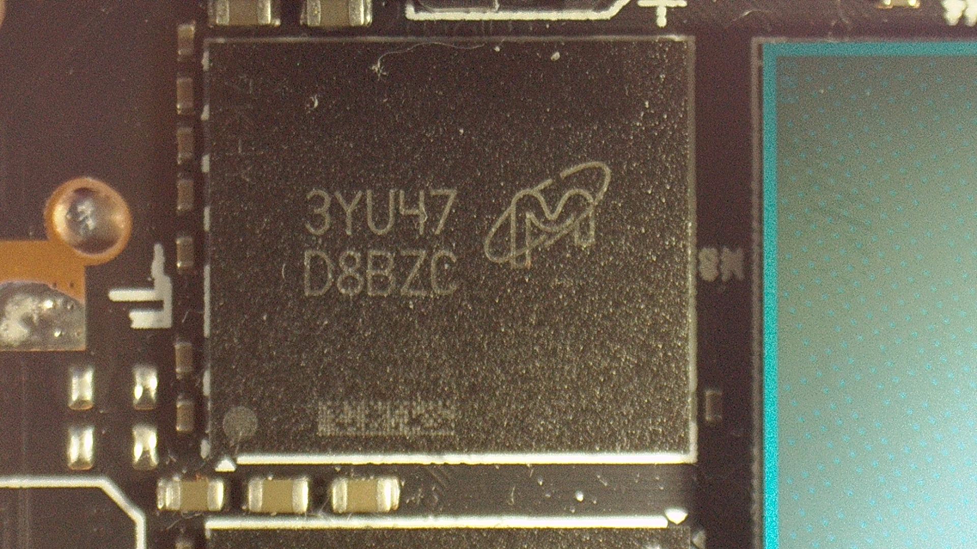
Let’s start with the PCB, which of course corresponds almost 1:1 to the PCB of the non-super with PNY. NVVDD is still the most important voltage and this results in a voltage converter design with a total of 8 real phases and the resulting 9 control loops for NVVDD alone, because one of the phases realizes parallel control of two regulators. Nothing has changed compared to the RTX 4070 Non-Ti, because in the end it is the same board. But it’s also about the price and so nothing else has changed. Fragmentation always costs extra and that doesn’t fit into the concept, here you can simply swap the chip and continue production as if the super upgrade hadn’t even happened.
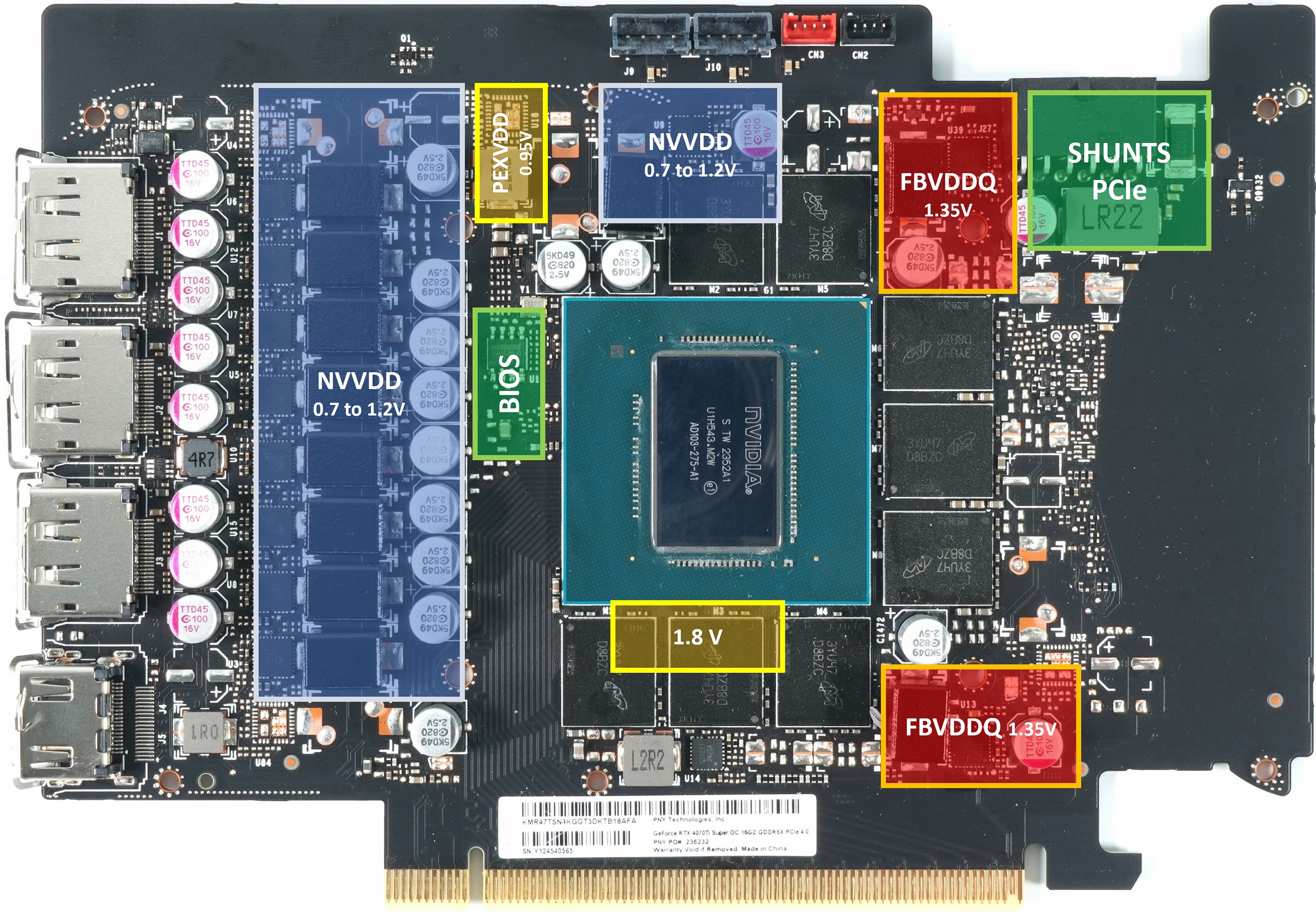
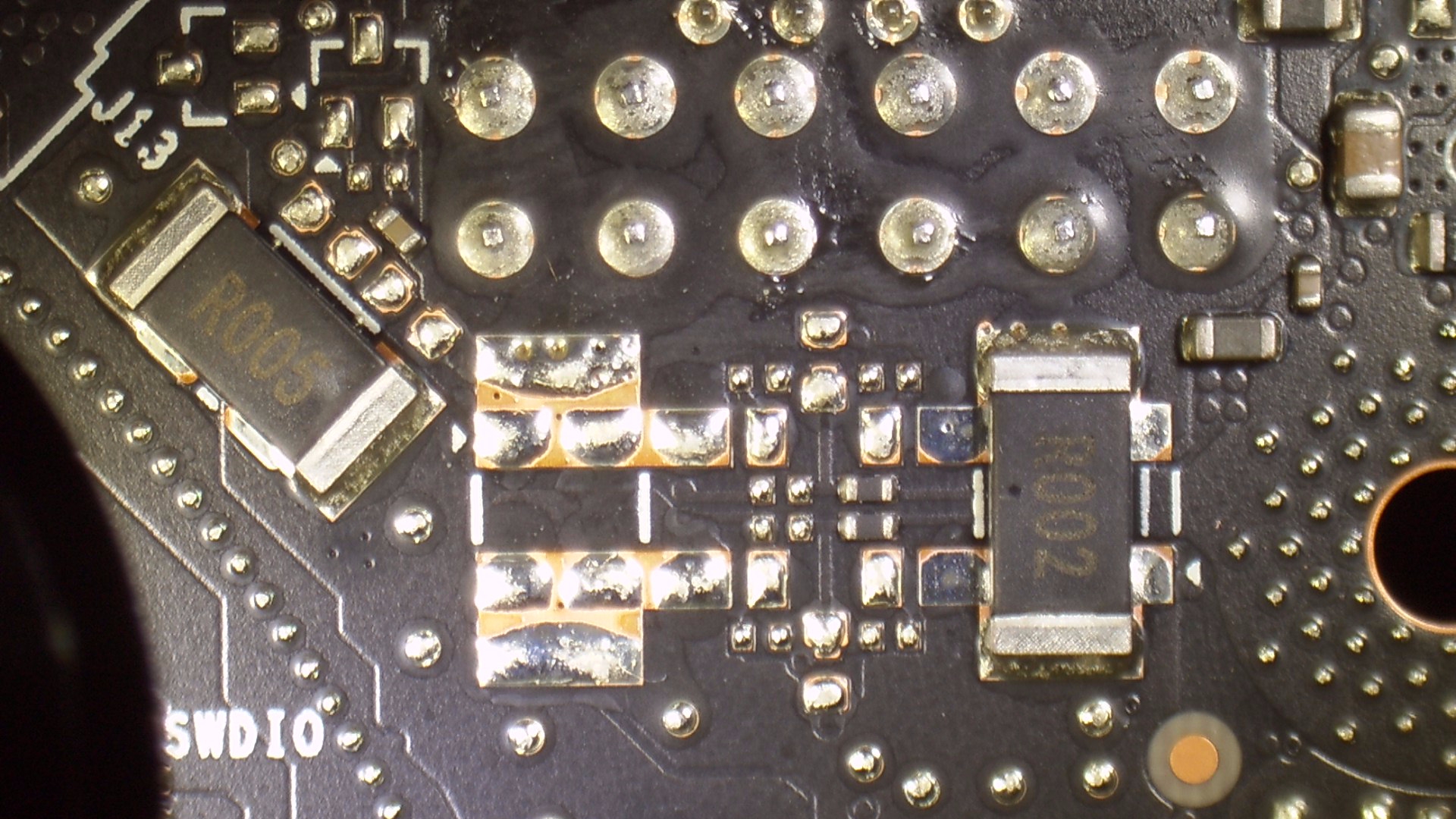
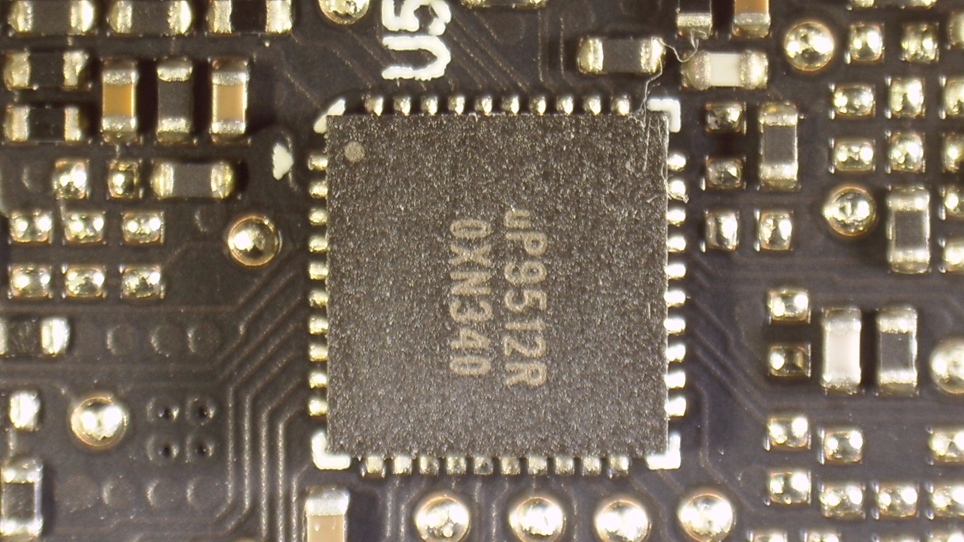
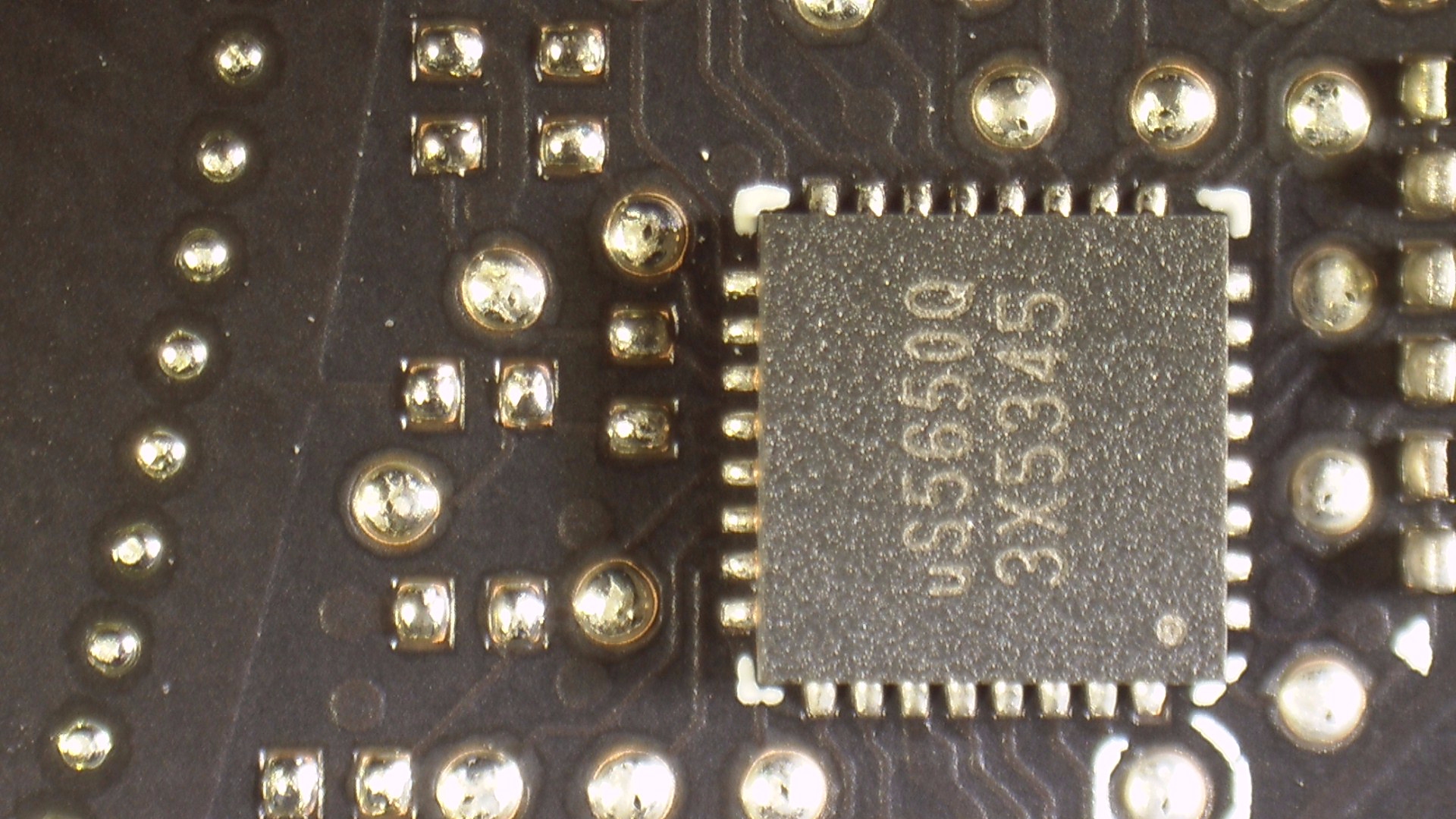
It doesn’t look as lean as the RTX 4070 Super, but the card is also thirstier and faster. Once again, separate PWM controllers are used for NVVDD (GPU core) and FBVDDQ (memory), as the top models among the PWM controllers are unfortunately far too expensive. Therefore, the good and well-known uP9512R from UPI Semi has to do the job again, but it is completely sufficient. A second PWM controller in the form of the small uP9529 is then used to control the two phases for the memory. Both controllers are located on the back of the board. Directly between them is a uPI uS5650Q for monitoring the 12V rails (1x Aux and 1x PEG). So there is no difference at all between the Super and Non-Super.
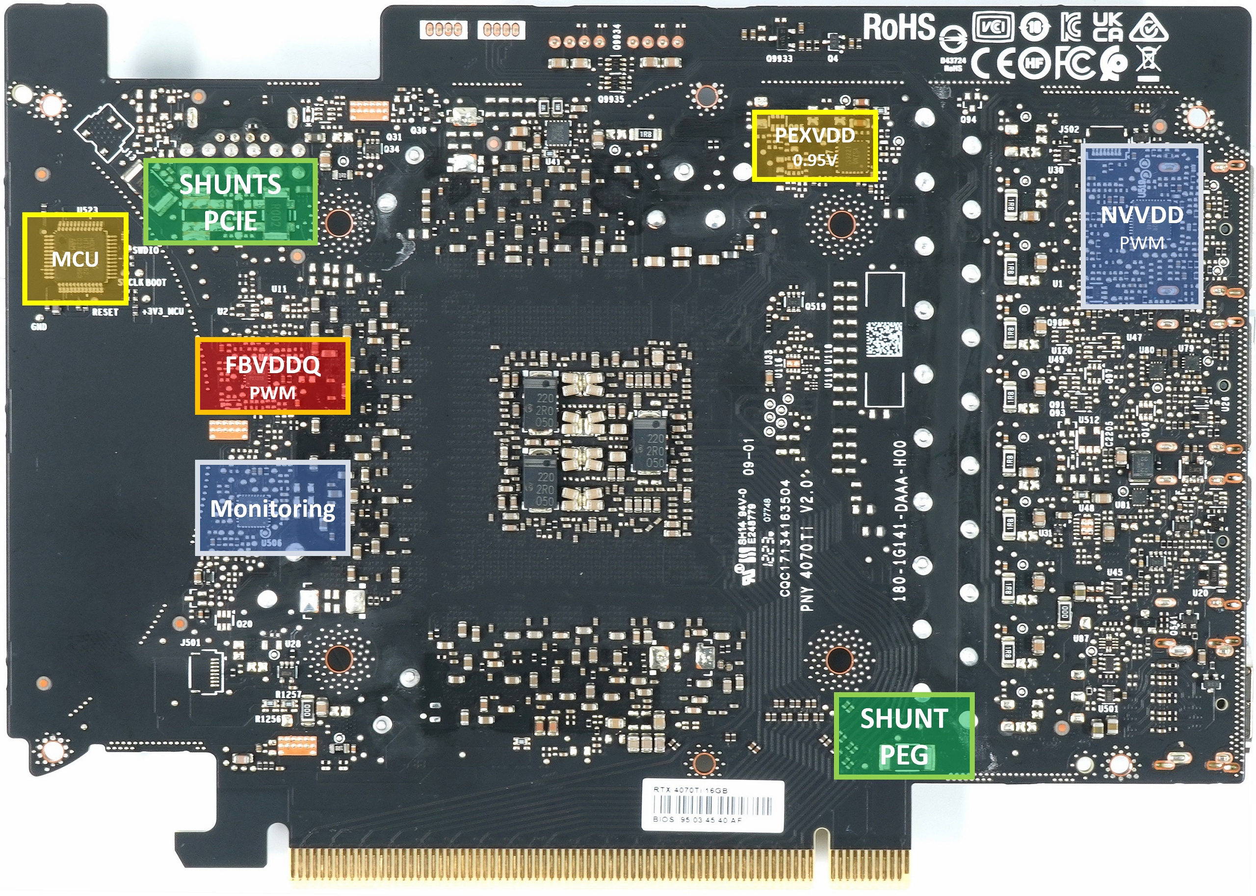
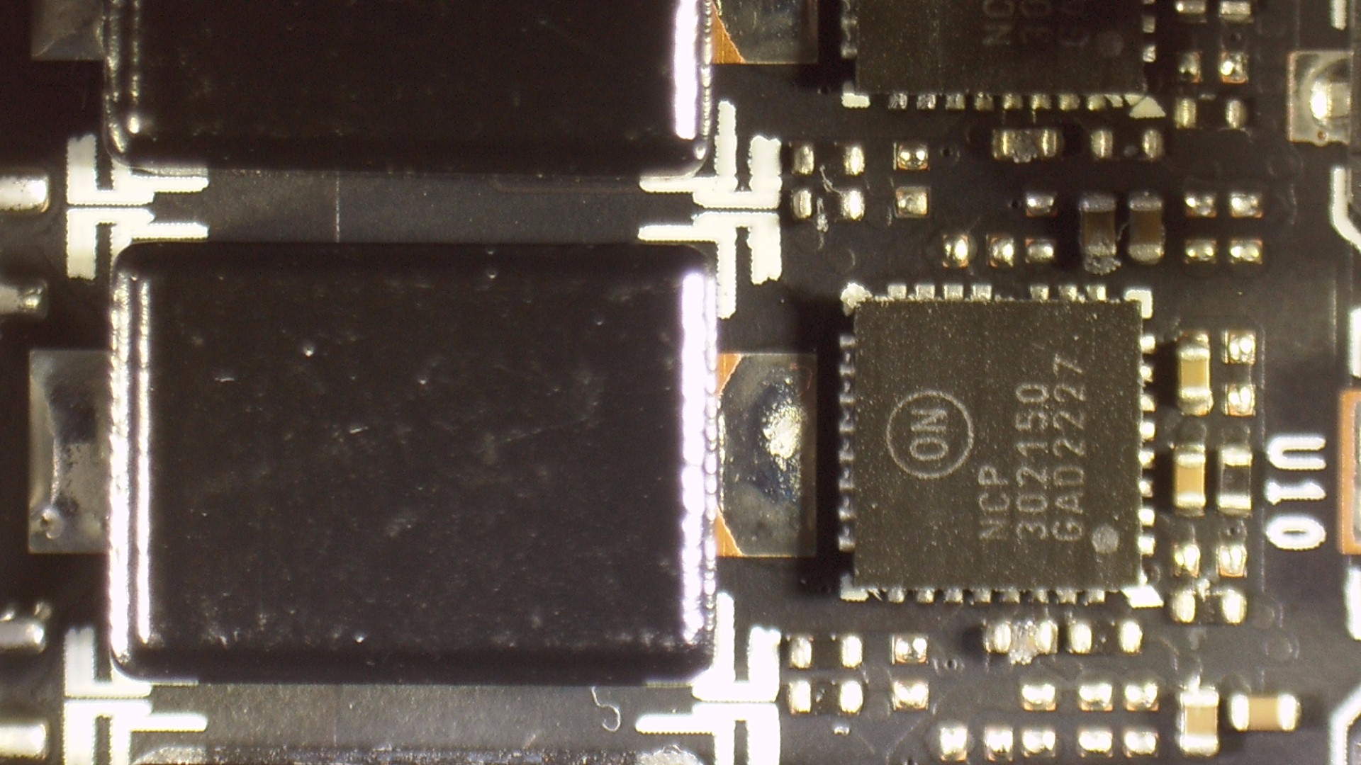
All DrMOS used, including those for the memory, are rather inexpensive products from OnSemi. The NPC302150 with 50A peak current used in all control circuits for NVVDD and FBVDDQ (memory) integrates a MOSFET driver, a high-side MOSFET and low-side MOSFET in a single package. This chip is specifically designed for high current applications such as DC-DC buck power conversion applications. This integrated solution reduces the footprint on the PCB compared to a solution with discrete components. The coils used for NVVDD and the memory have an inductance of 220 nH, the capacitors are in cup form, which is more favorable.
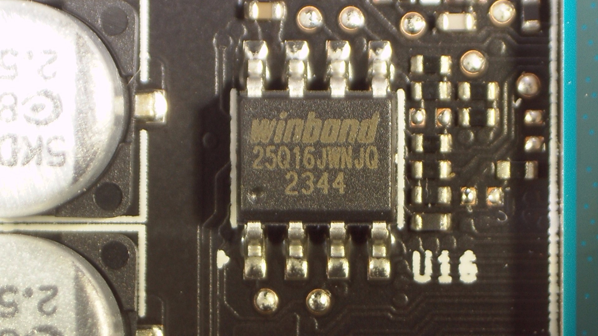
The 12V rails on the 12 4 12VHPWR connector are combined into a single rail directly after the socket, another is connected to the PEG and is only used slightly for NVVDD. The BIOS is in the usual place and the generation of the remaining extra-low voltages is the same as before. So there are no more special features.
- 1 - Introduction, technical data and technology
- 2 - Test system and measuring equipment
- 3 - Teardown: Cooler
- 4 - Teardown: PCB, layout and components
- 5 - Teardown: Detailed material analysis
- 6 - Gaming Performance FHD (1920 x 1080)
- 7 - Gaming-Performance WQHD (2560 x 1440)
- 8 - Gaming Performance Ultra-HD (3840 x 2160)
- 9 - Gaming Performance DLSS / FSR
- 10 - Power consumption and load balancing
- 11 - Load peaks, clipping and PSU recommendation
- 12 - Temperatures, clock rates and infrared analysis
- 13 - Fan curves and noise level with audio sample
- 14 - Summary and conclusion


123 Antworten
Kommentar
Lade neue Kommentare
Veteran
Mitglied
1
1
Urgestein
Veteran
Urgestein
Urgestein
Urgestein
Urgestein
Urgestein
Urgestein
1
1
Urgestein
Mitglied
1
Urgestein
Urgestein
Alle Kommentare lesen unter igor´sLAB Community →