


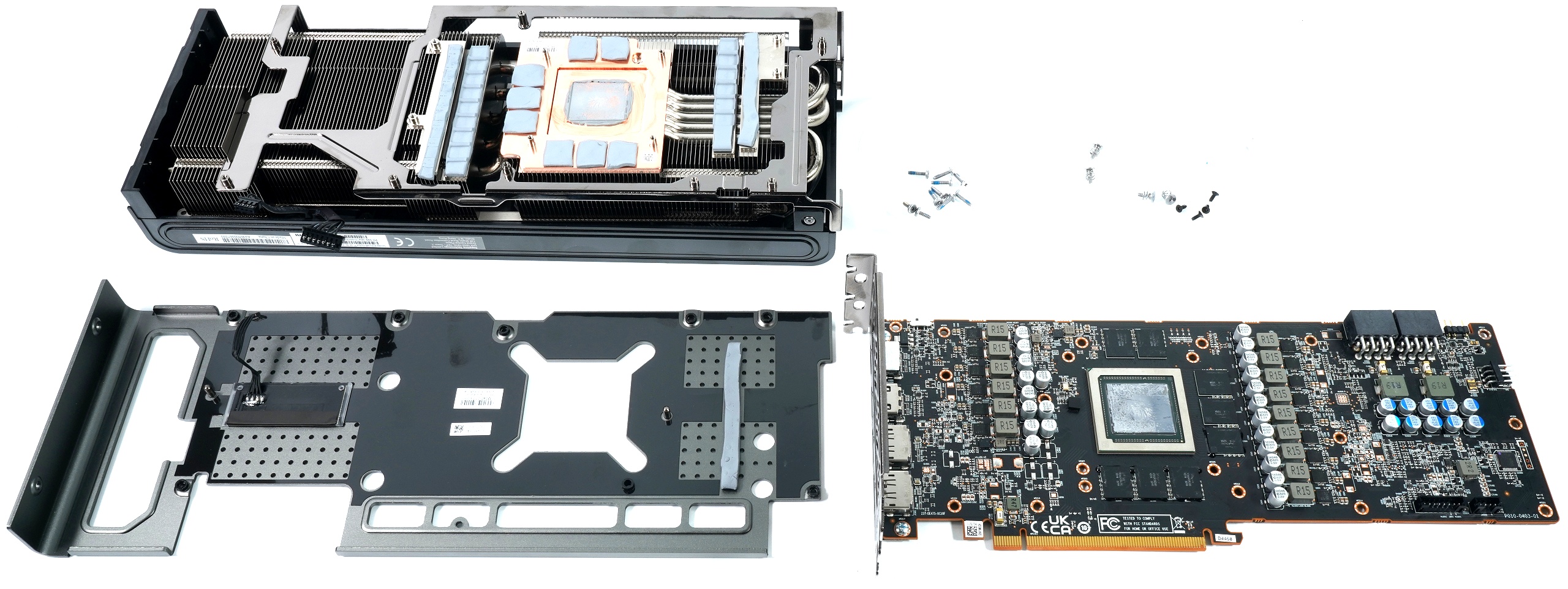
Teardown and disassembly
The structure of the cooler is much more detailed than that of the cooler on the large VaporX. But with a little logic, everything can be solved here too, in the truest sense of the word. Nevertheless, I would always recommend using very good tools, as the screw heads of the clamping cross in particular are somewhat soft.
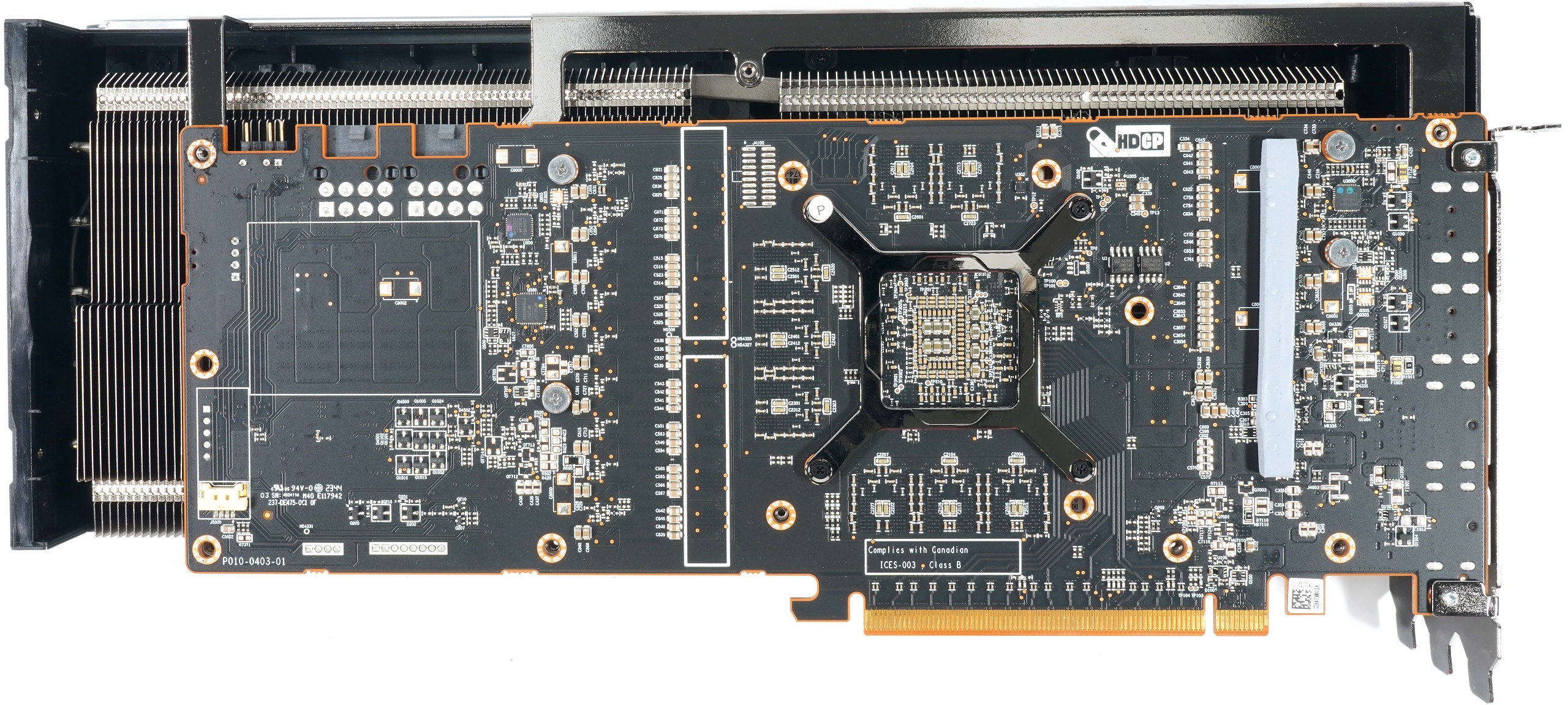
Two hexagon socket screws at the end of the card additionally secure the backplate, but also need to be operated properly with tools. The time required is approximately 5 minutes without cleaning the components.
PCB layout and components
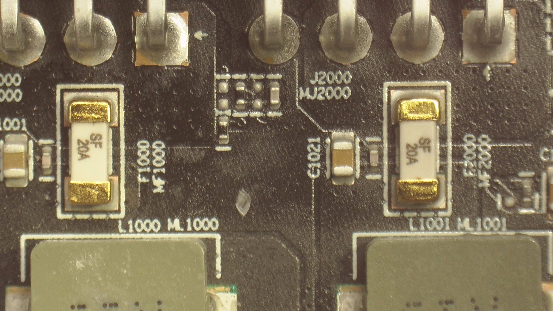
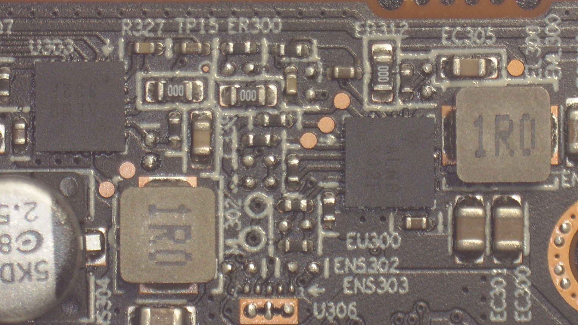
In principle, the GRE PCB is a slightly simplified version of the XT PCB. Here, too, we find VDDCR_GFX. Instead of the 10 phases of the XT, only 9 are used, each of which then controls a single voltage regulator. VDD_SoC remains with 2 phases and one voltage regulator per phase, as well as VDDCR_USR with 1 phase and therefore only one voltage regulator. In addition, there are the 2 phases or 2 voltage regulators for VDD_MEM (XT 3 each) and a single buck converter for VDDCI_MEM.
Although the generation of VDDCI_MEM is not a large item in terms of performance, it is extremely important. It is used for the GPU-internal level transition between the GPU and the memory signal, something like the voltage between the memory and the GPU core on the I/O bus. In addition, a constant source for 0.75 volts is generated. The majority of these very similar voltage converters are located on the front of the board. There is also a 1.8V source (TTL, GPU GPIO), VDD_13 (Aux) and an ultra-low dropout chip generates the very low voltage for the PLL area (VPP).
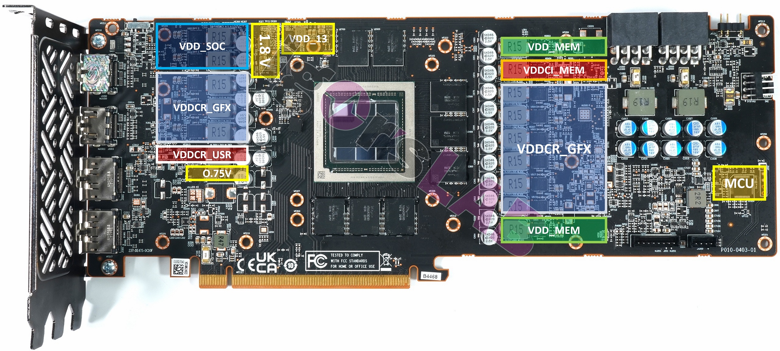
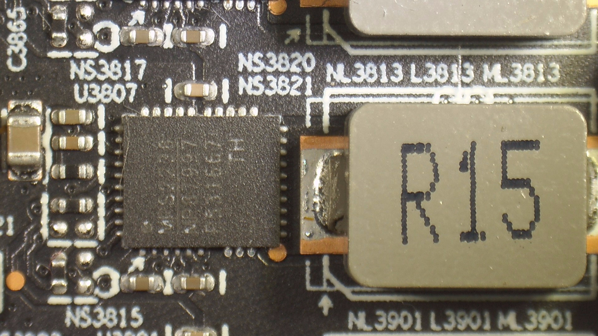
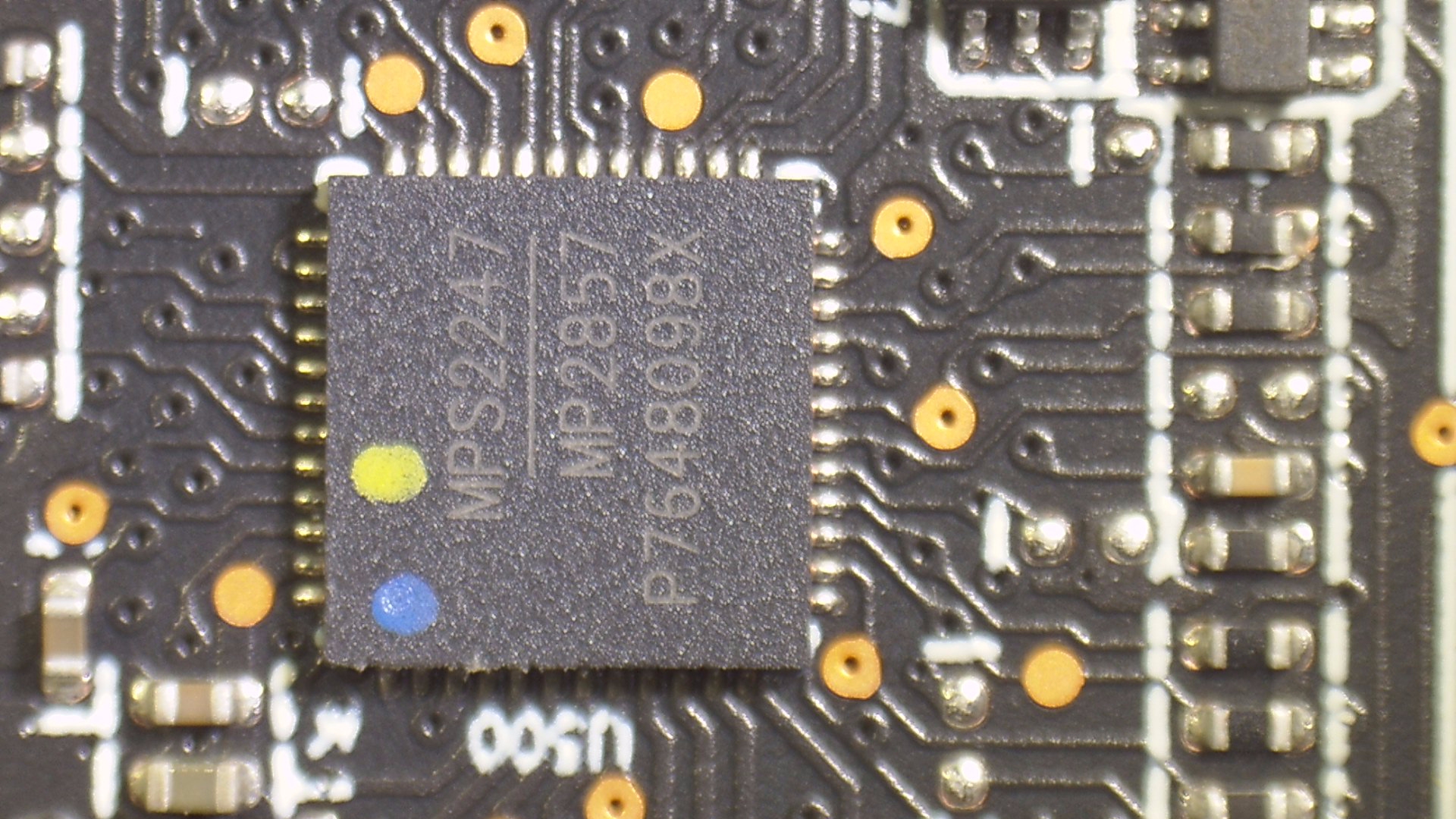
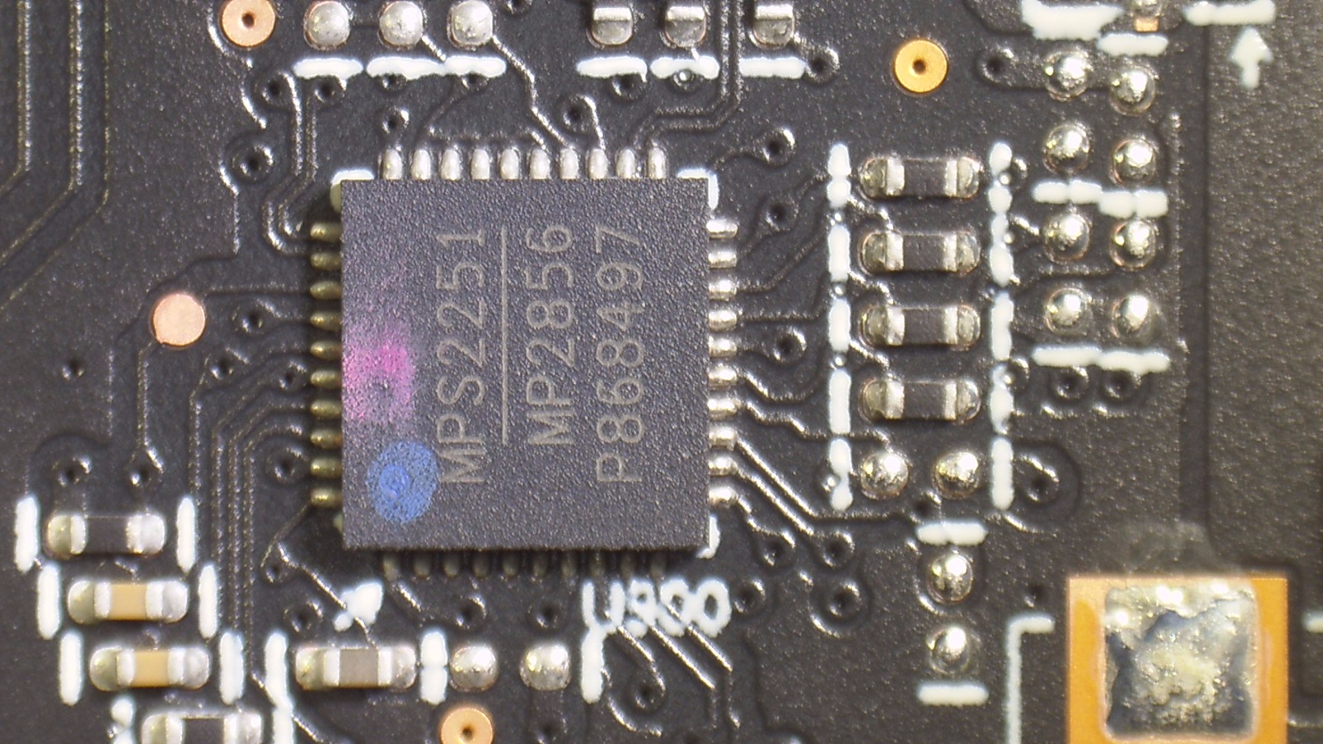
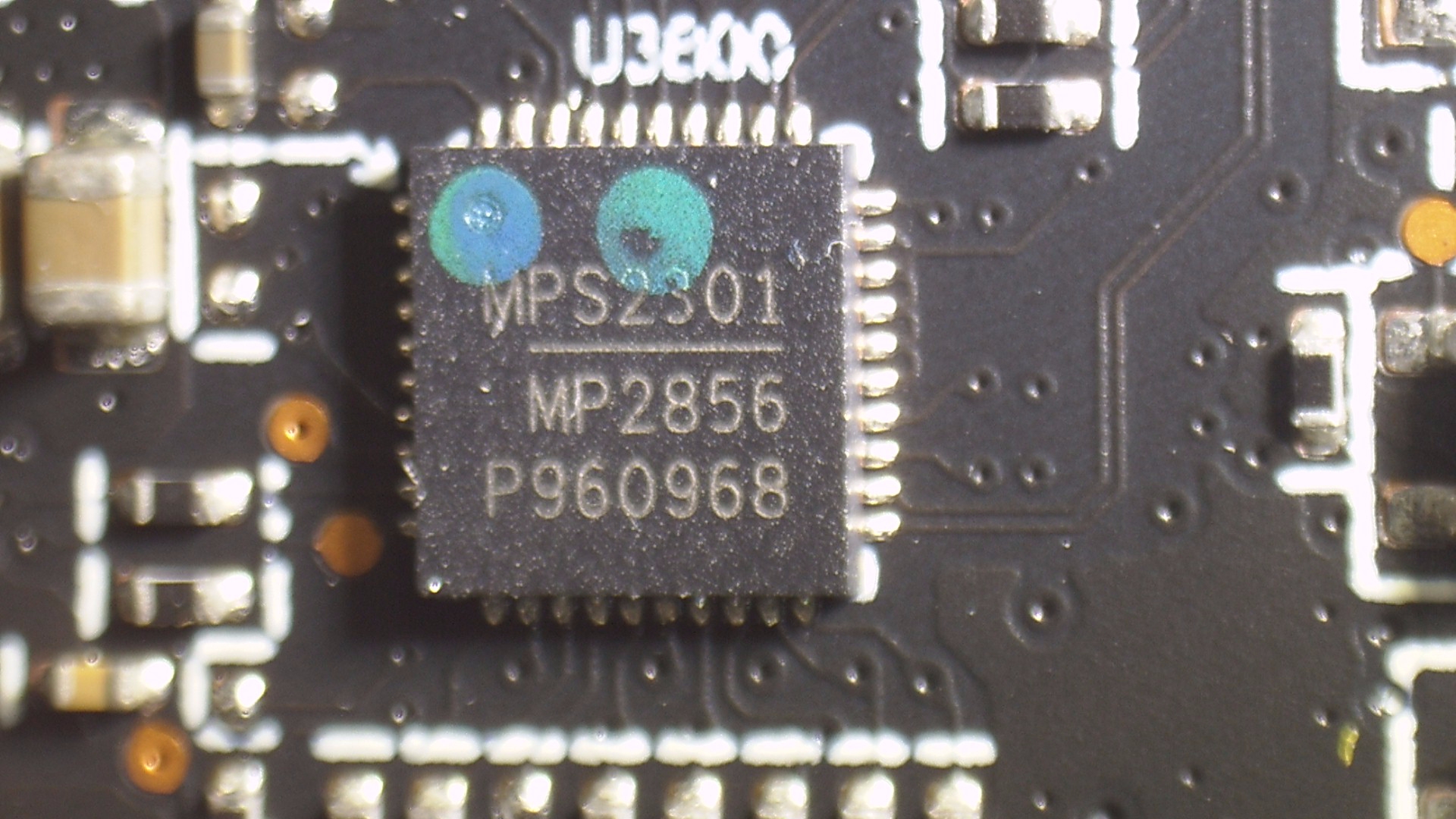
Two PWM controllers for generating the most important phases are located in the upper left third of the back of the board, with another in the upper right. This time, AMD relies on the top products from Monolith, as did NVIDIA for the reference cards. The first rail of the MP2857 is used for the 9 phases of the VDDCR_GFX, while the second rail is used to generate the VDD_MEM. It is a digital, multiphase dual-rail controller that primarily provides the power supply for the PWM VID core and is also compatible with the AVS bus interface.
The MP2857 can (and should) also work with Monolith’s Intelli-Phase products to complete the multiphase voltage regulator (VR) solution with a minimum of external components. The two somewhat smaller MP2857s, which unfortunately are also not publicly available in terms of data, are then responsible for VDDCI, VDD_SoC and VDDCR_USR, depending on the side.
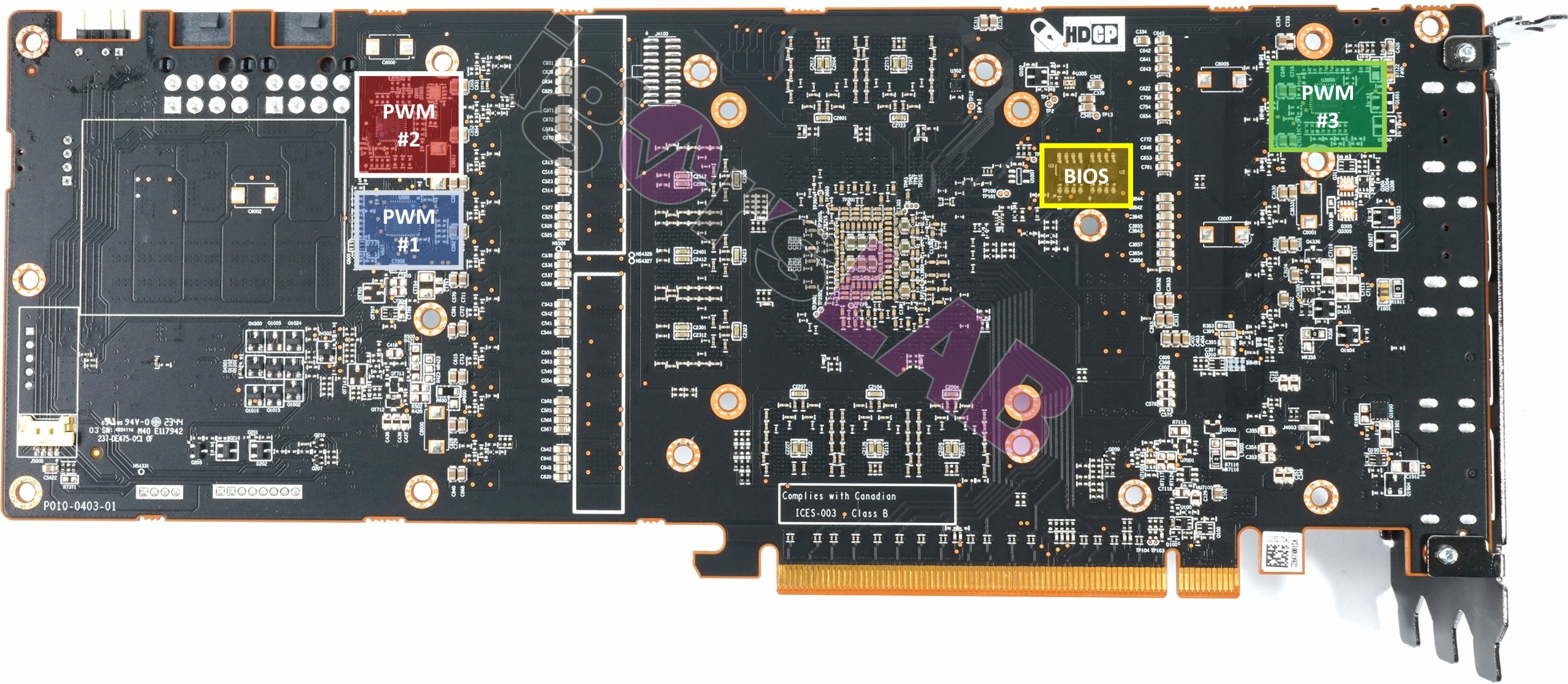
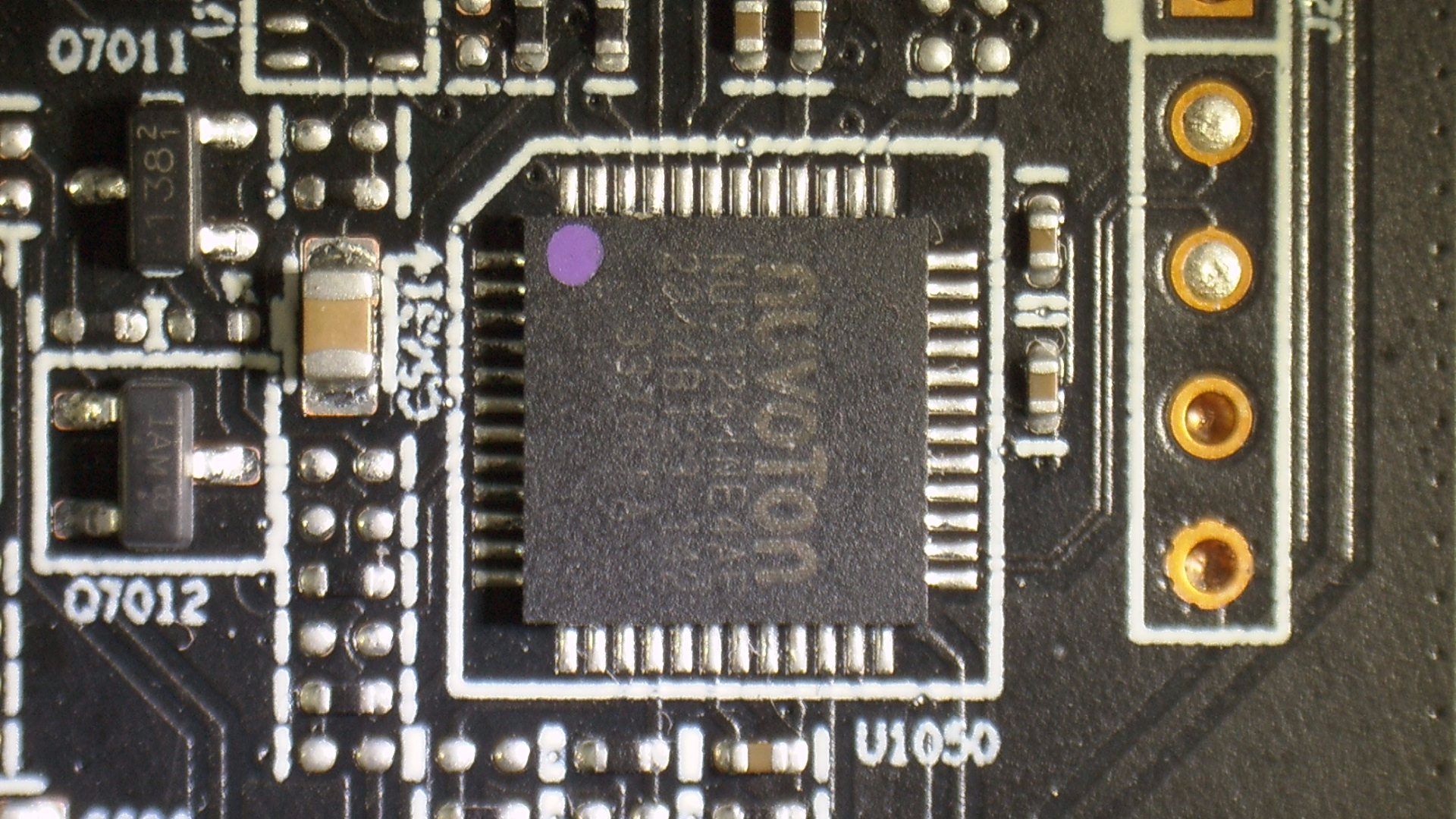
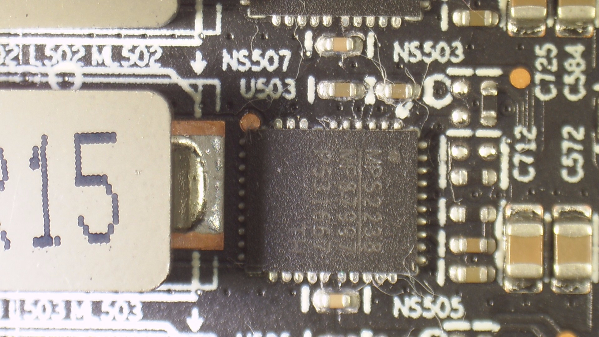
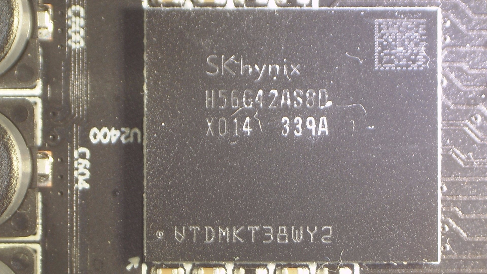
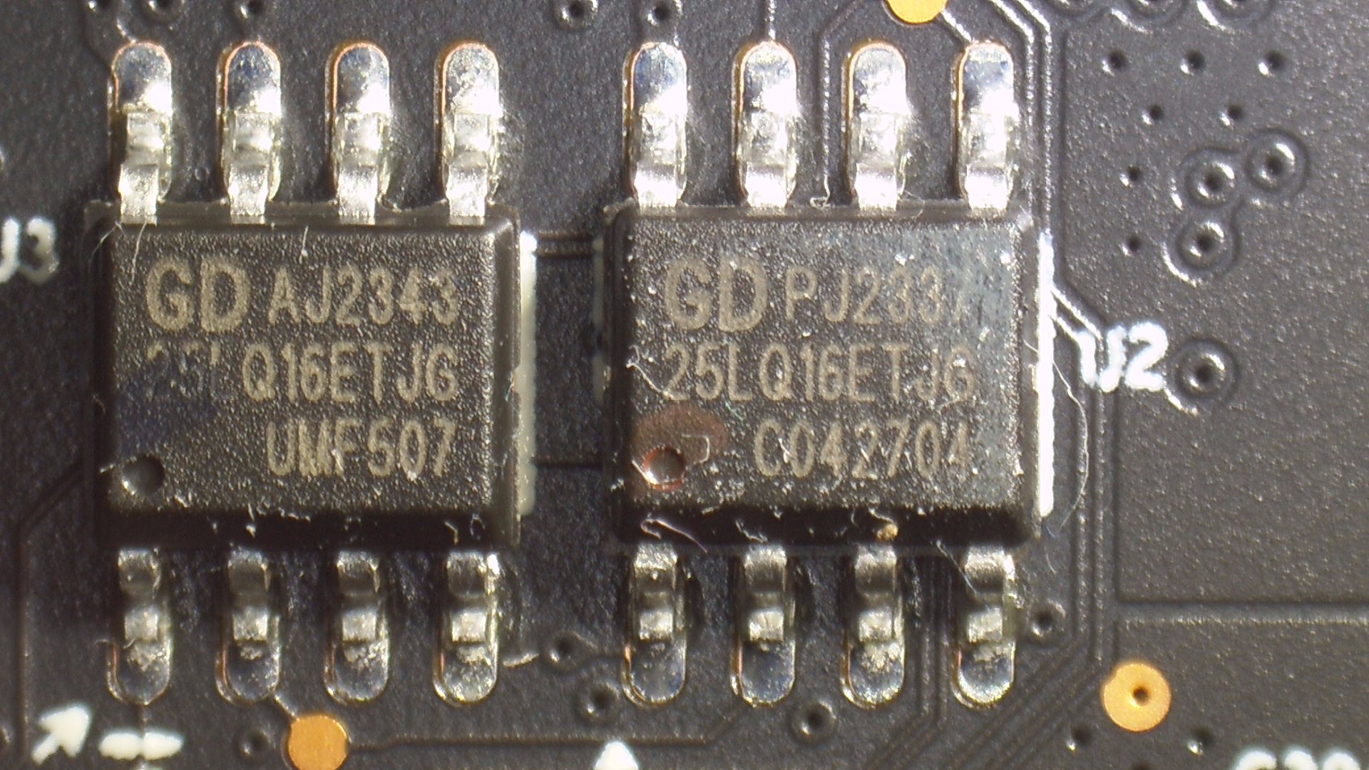
All power stages used, including those for the memory, are also products from Monolith. The MP87997 is also not freely documented, but it should be a very powerful monolithic half-bridge. The integration of drivers and MOSFETs (DrMOS) results in high efficiency due to an optimized dead time and a reduction of parasitic inductance. This small, 5 mm x 6 mm LGA component fits perfectly with the MP2857 and MP2856. The MCU for all the control tasks comes from Nuvoton, and of course we also have the eight RAM modules from SK hynix with the 18 GT/s.

- 1 - Introduction, technical data and technology
- 2 - Test s4etup and methods
- 3 - Teardown: PCB and components
- 4 - Teardown: cooler and cleaning tips
- 5 - Teardown: material analysis
- 6 - Gaming-Performance Full-HD (1920 x 1080)
- 7 - Gaming-Performance WQHD (2560 x 1440)
- 8 - Gaming-Performance Ultra-HD (3840 x 2160)
- 9 - Gaming-Performance DLSS / FSR (3840 x 2160)
- 10 - Gaming-Performance FSR3 Frame Generation (3840 x 2160)
- 11 - Latenzen
- 12 - Power consumption and balancing
- 13 - Transients and PSU recommendation
- 14 - Temperatures, IR analysis and clock rate / OC
- 15 - Fan curves, noise and audio sample
- 16 - Summary and conclusion


299 Antworten
Kommentar
Lade neue Kommentare
Urgestein
1
1
Urgestein
Urgestein
Urgestein
Mitglied
Urgestein
1
Urgestein
Veteran
Mitglied
Urgestein
1
Urgestein
Urgestein
Veteran
Urgestein
Mitglied
Alle Kommentare lesen unter igor´sLAB Community →