


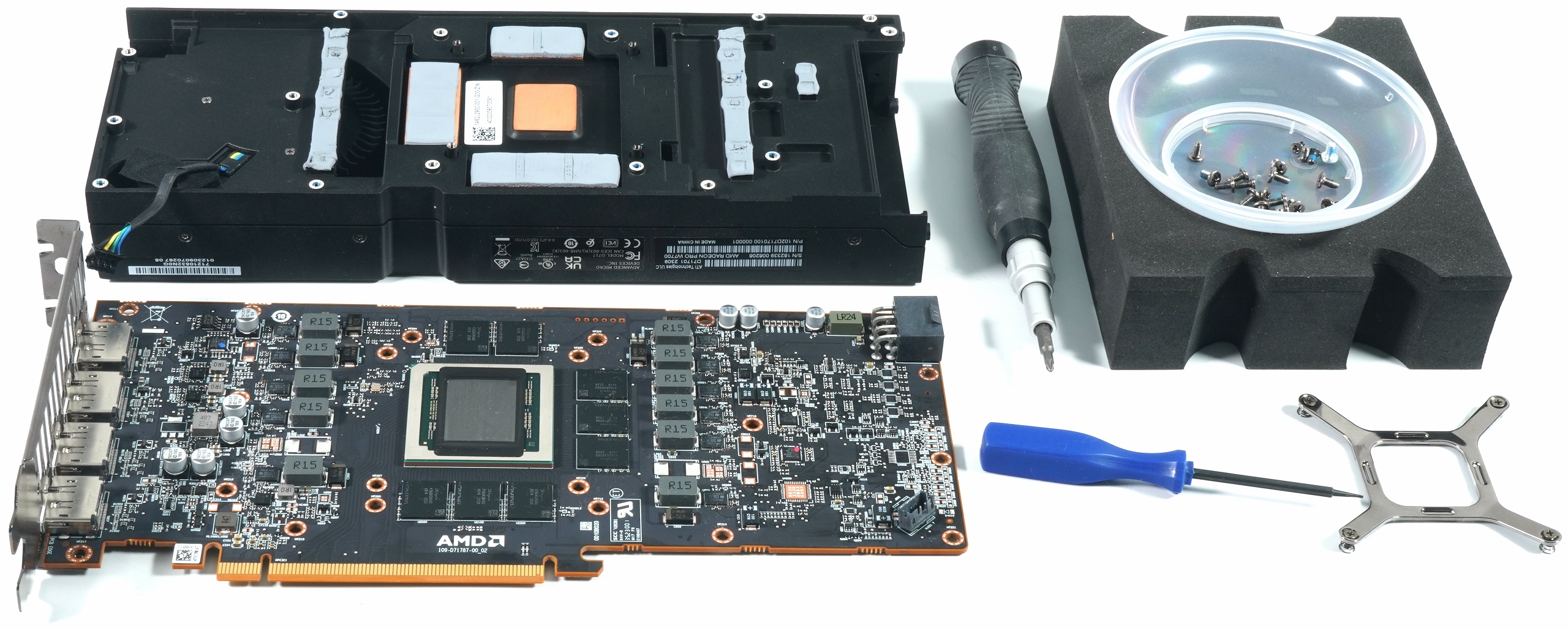
Disassembly and teardown
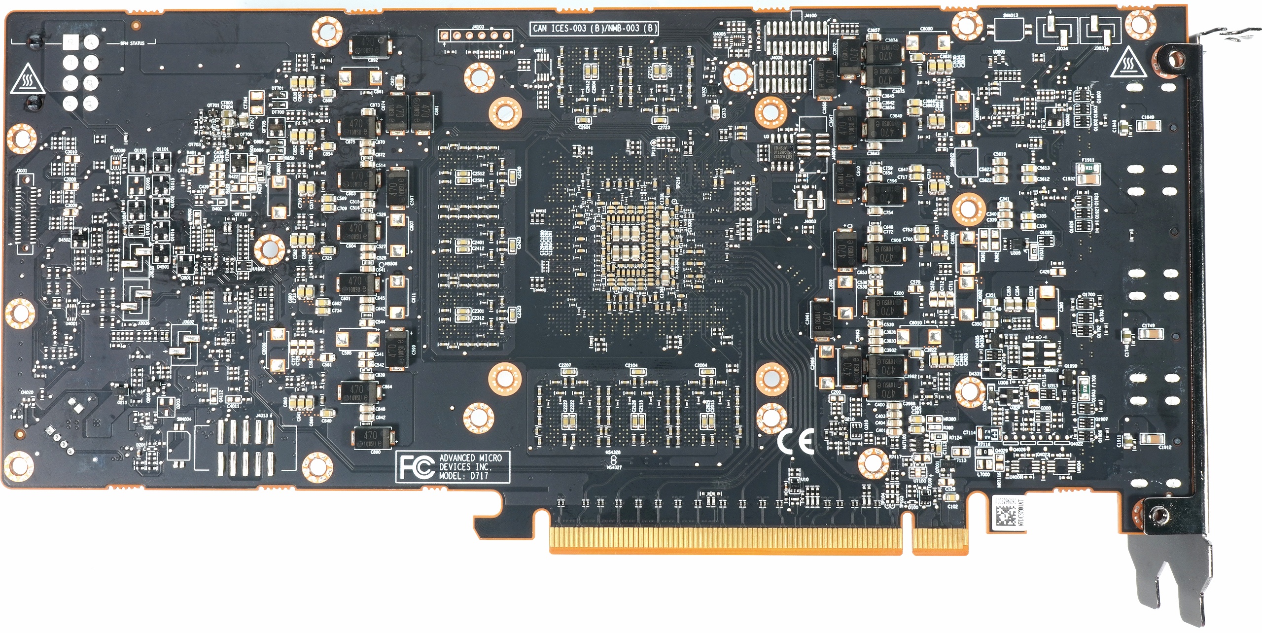
Disassembly is part of an objective review and without this action and the subsequent board and cooler analysis, you unfortunately never really reach your goal. For this very reason, I have of course made an effort to reassemble the card true to the original after the analysis. The material analysis is particularly interesting (next page). And the circuit also has to be explained, because unfortunately very few people do. The PCB from SHEN NAN CIRCUITS CORP LTD is very similar to the reference PCB of the RX 7800XT in terms of the voltage converter topology, even if there were some major repositioning in places due to the design.
PCB layout and components
So let’s get straight to the PCB analysis. And this is where I need and want to give you a few details that are fundamentally different for AMD than for NVIDIA. Anyone can count phases (or at least thinks they can), but this is a little misleading. This is because AMD uses three expensive dual-rail PWM controllers to generate the five (!) most important voltages, as well as real Smart Power Stages (SPS), which can report back the flowing currents (IMON) and temperatures (TMON) in real time. This makes telemetry happy, because AMD doesn’t go NVIDIA’s simple way with the shunts to monitor the power limit of the entire card including all losses BEFORE the voltage converters (primary side), but controls all the currents individually directly AFTER the voltage conversion.
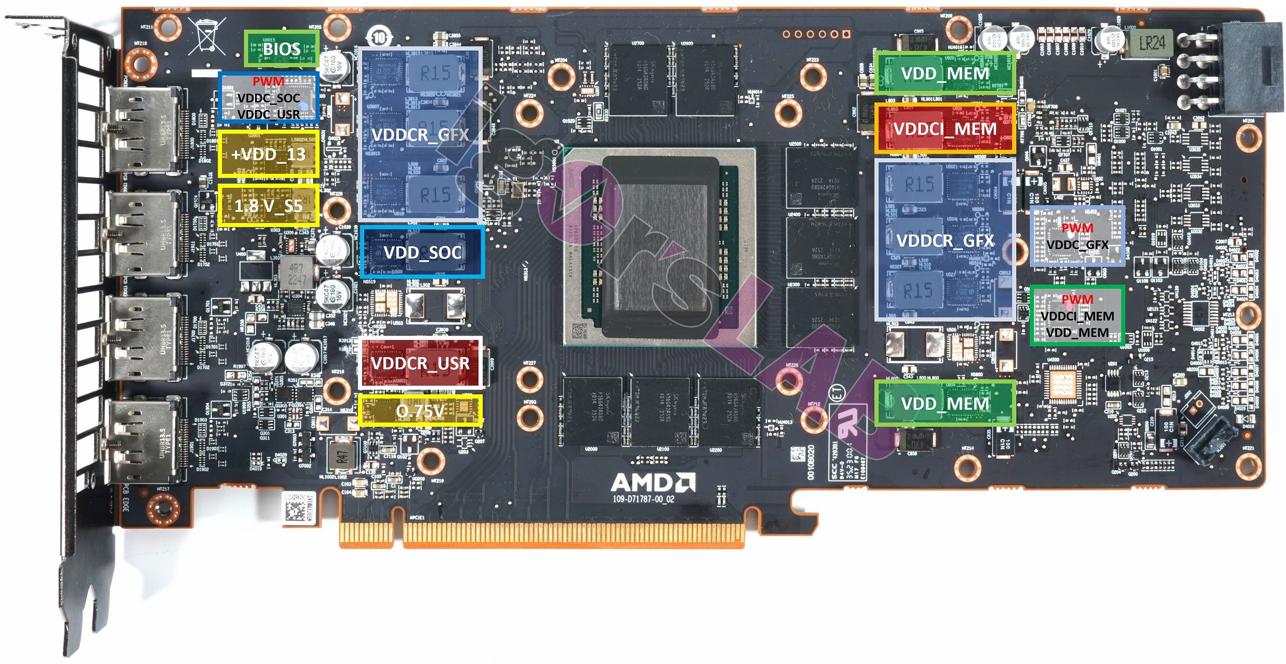
As questions have repeatedly been asked as to which voltages these are in detail, I will explain the less well-known voltages today. The acronym “VDD” stands for “Voltage Drain-Drain”, which comes from MOSFET terminology, and is used to describe the supply voltage. This term will come up again and again, so I’d better explain it in advance. And now let’s go into the details of the “magic five”.
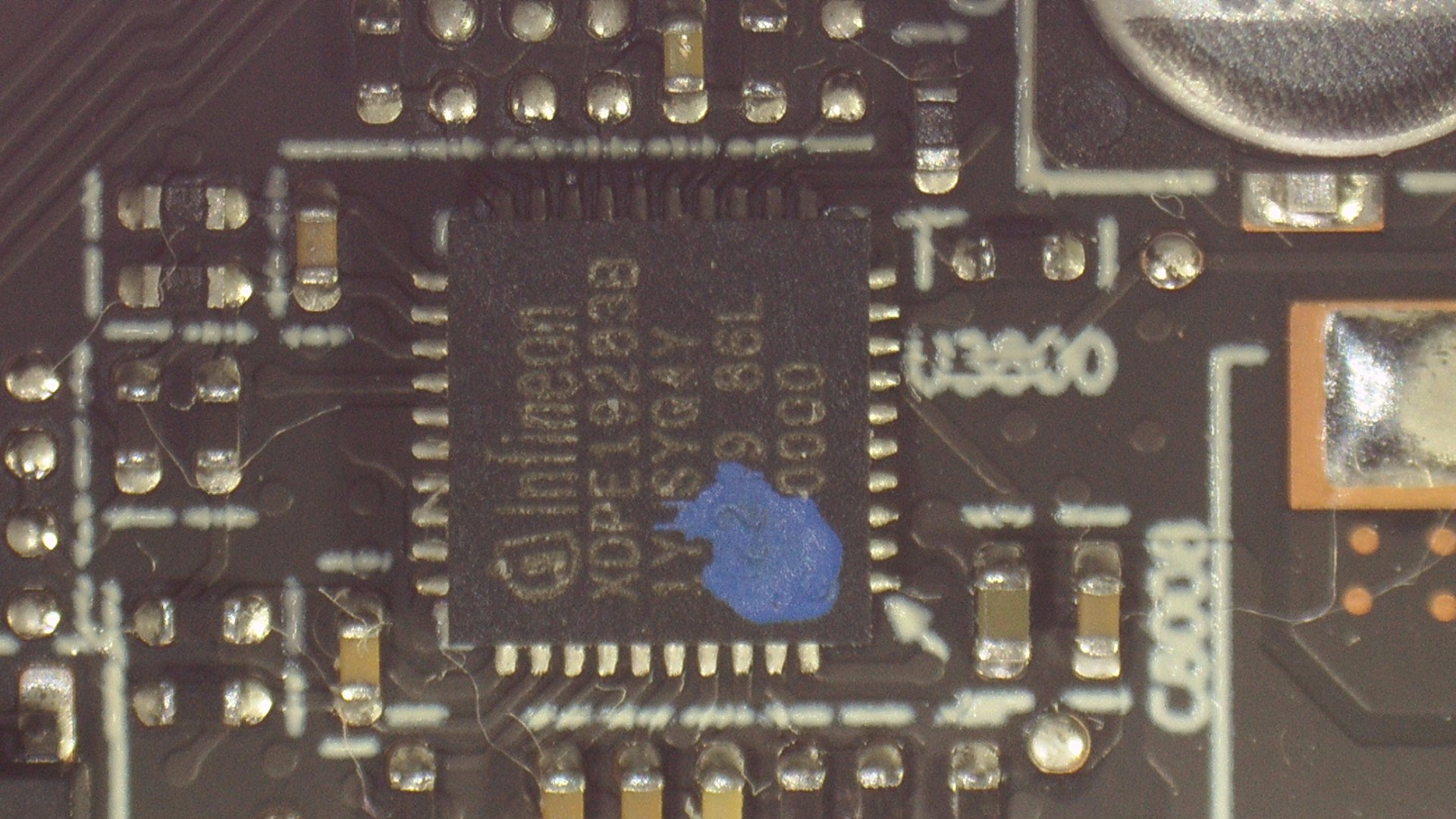
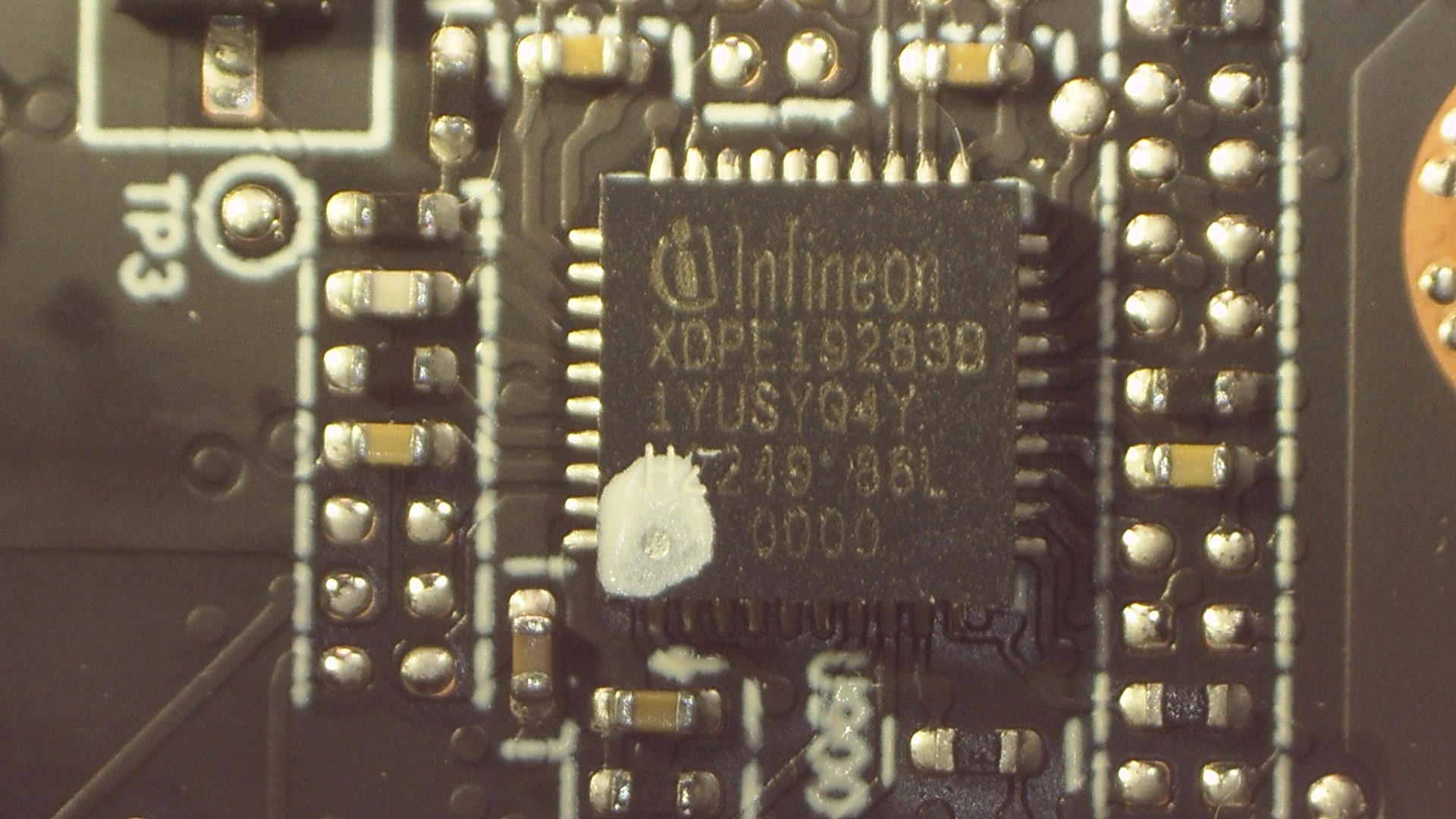
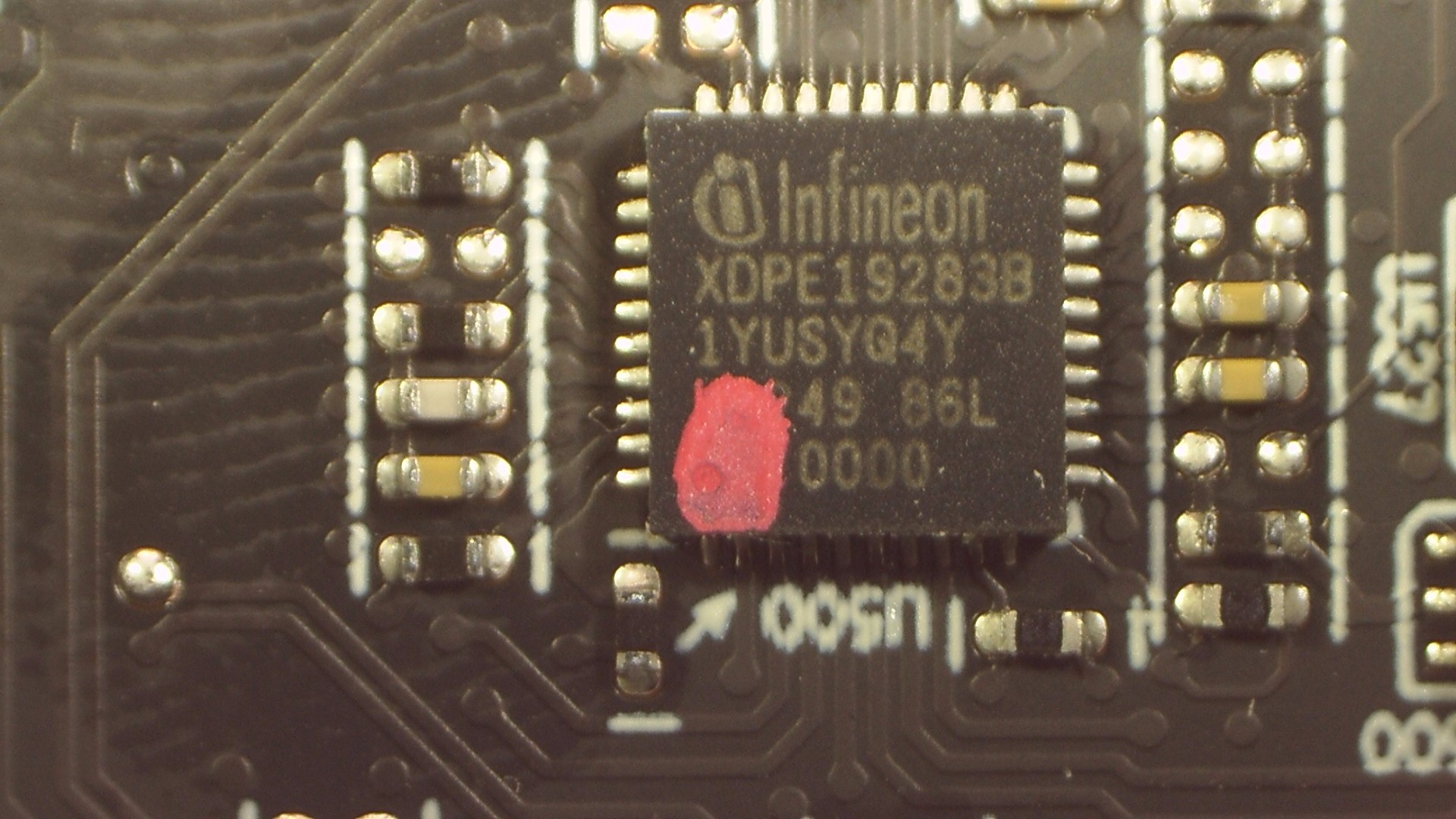
The power supply naturally relies on VDDCR_GFX (i.e. the equivalent of NVIDIA’s NVVDD) as the largest item for the GPU. AMD only uses six phases here, each of which controls a single PLC (voltage regulator). The board would allow for more phases, but the Infineon XDPE192838 controller is used, which could handle significantly more phases and can communicate with AMD’s SVI2 interface. It is a digital, multi-phase controller that primarily provides the power supply for PWM VID cores and is also compatible with the AVS bus interface. It can also work with Infineon’s Smart Power Stages (SPS) to implement the multiphase voltage regulator (VR) solution with a minimum of external components. This is why the PMC41420 from the same manufacturer is used as the Smart Power Stages (SPS).
Another PWM controller of the same type controls one phase for VDD_SOC and one for VDD_USR. VDD_SOC writes the supply voltage level that drives the system-on-chip. This voltage level is important to the operation of the SoC and must be precisely specified and regulated to ensure that the chip functions properly. Even more mysterious, however, is VDD_USR. The USR stands for Ultra-Short Reach and should actually be called USR_PHY. This is because it is a voltage for inter-die communication and PHY stands for the physical layer of a connection protocol. In short, the MCM components of the chiplet design also want and need to exchange data with each other.
Below the PWM controller for VDDCR_GFX is the PWM controller for the voltage supply of the VDD_MEM and VDDCI_MEM memory. Here (as with VDD_USR and VDD_SOC) a cheaper model would have been sufficient, but the large controller is also fitted. VDDCI_MEM is not a big item in terms of performance, but it is extremely important. It is used for the GPU-internal level transition between the GPU and the memory signal, something like the voltage between the memory and the GPU core on the I/O bus.
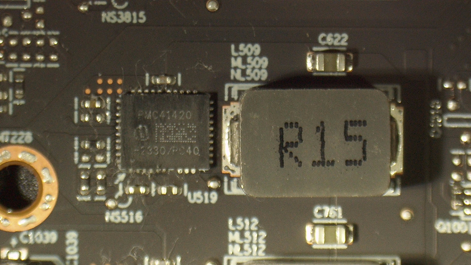
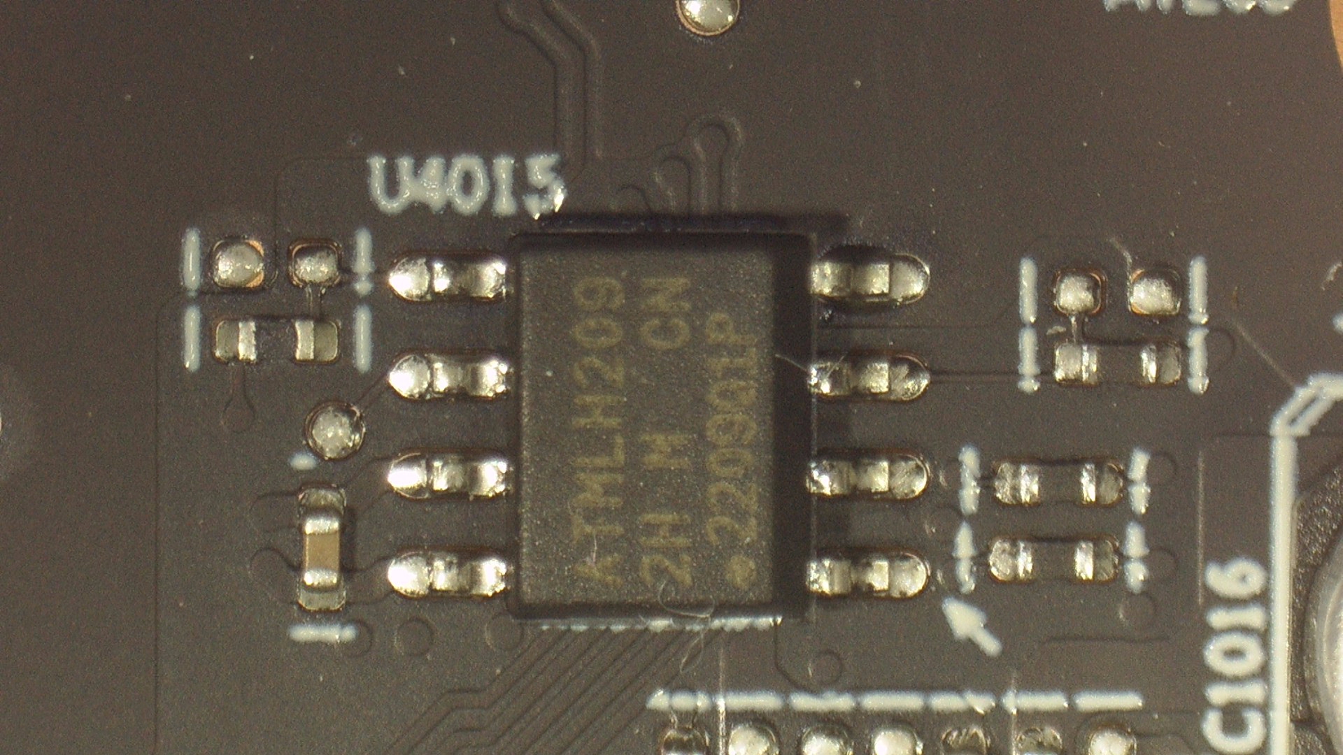
The majority of these very similar voltage converters are located on the front of the board. There is also a 1.8V source (TTL, GPU GPIO), VDD_13 (Aux) and an ultra-low dropout chip generates the very low voltage for the PLL area (VPP). All the power stages used, including those for the memory, are again the same Infineon products. The PMC41420 used throughout is a very powerful monolithic half-bridge and the integration of drivers and MOSFETs (DrMOS) results in high efficiency due to optimal dead time and a reduction in parasitic inductance.
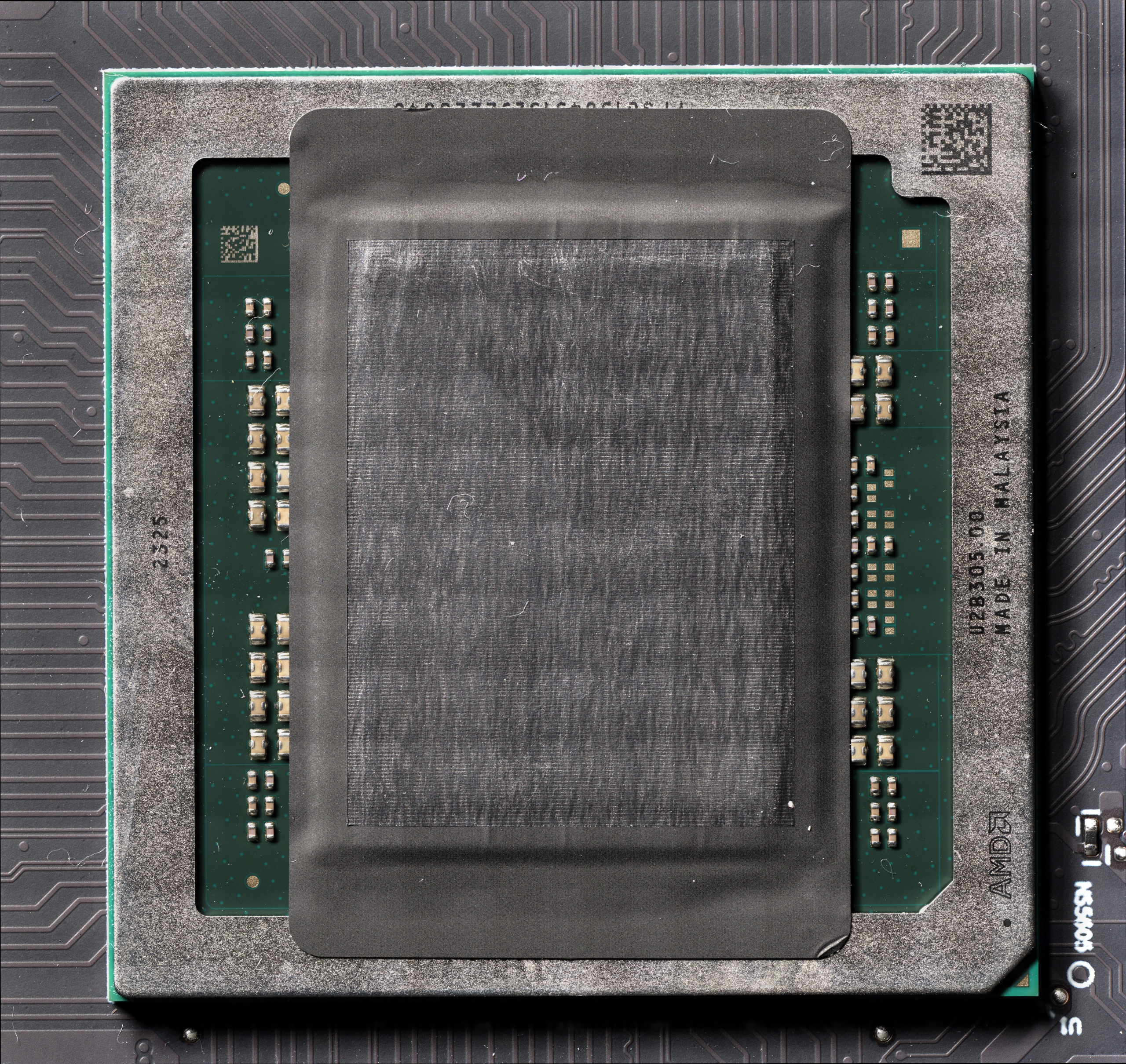
Package and thermal pad
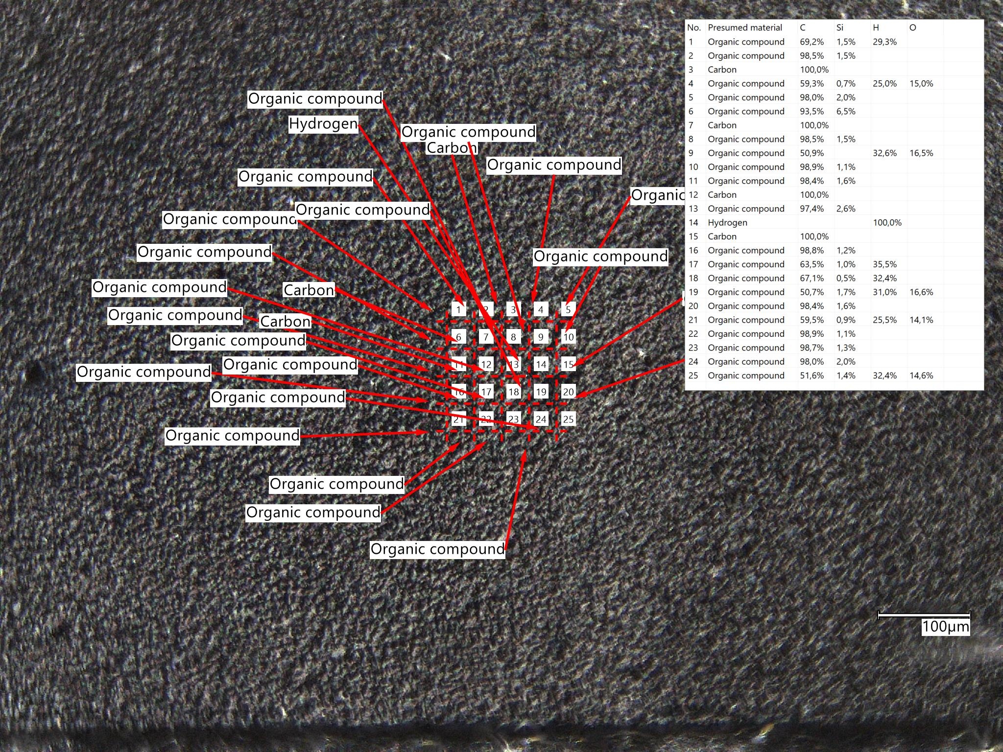
Here we come to a special feature and yes, AMD continues to learn. A completely new type of thermal pad is used and I suspect, also based on the material analysis, that it is made of graphane instead of the usual graphene. In favor of graphane instead of graphene is the fact that the pad has been placed over SMD components without any worries, because the pure graphite or graphene pads are electrically conductive. So the material analysis has to be right. However, we can also see that it is also a type of phase change pad with burn-in.
Graphane, a material that is closely related to graphene, can be produced by interacting with atomic hydrogen. This atomic hydrogen is produced by means of an electrical discharge in a hydrogen-argon mixture. In this process, each carbon atom of graphene is bonded to a hydrogen atom, creating graphane. The resulting bond structure of graphane resembles the chair-shaped structure of cyclohexane. Interestingly, this hydrogen bonding fundamentally changes the electronic properties of the original material. While graphene is an excellent electrical conductor, graphane becomes an electrical insulator. This property makes graphane particularly interesting for applications in electronics, for example in the development of transistors and sensors, or for electrically insulating thermal pads.
And because we are so busy analyzing, the cooler is also available on the next page.


17 Antworten
Kommentar
Lade neue Kommentare
Urgestein
Veteran
Urgestein
Urgestein
Urgestein
Urgestein
Urgestein
Veteran
Urgestein
Mitglied
Urgestein
1
Urgestein
Veteran
Urgestein
Alle Kommentare lesen unter igor´sLAB Community →