


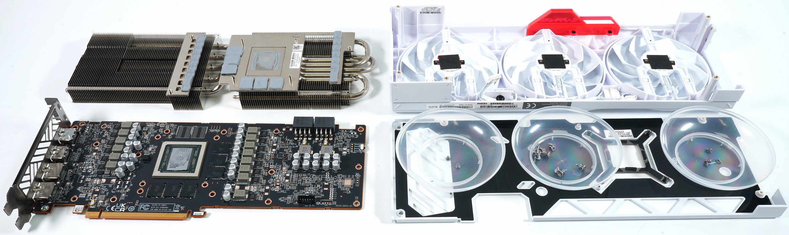
Disassembly and Teardown
Sapphire has nothing against disassembling and yes, without this action, the following board and cooler analysis as well as a real 3D scan, you will unfortunately never reach your goal. Exactly for this reason, I of course made an effort to reassemble the card true to the original after the analysis. Especially the material analysis is quite interesting (next page). And the circuit has to be explained, because unfortunately very few people do that.
The board of the Sapphire card is largely identical to the reference board in terms of voltage converter topology, but still has a free area for an MCU and expandable RGB stuff, which is not used in the Pure, though. In addition, the lower four RAM modules still have an underfill, which the other cards do not have. The rest is again like the MBA.
PCB layout and components
Now we come directly to the PCB analysis. And exactly here I have to and want to give you a few details, which are solved basically differently with AMD than with NVIDIA. Everyone can count phases (or at least believes it), but that’s even a bit misleading here. AMD uses three expensive dual-rail PWM controllers for the generation of the five (!) most important voltages and also real Smart Power Stages (SPS), which can report the flowing currents (IMON) and temperatures (TMON) in real time. Telemetry is happy about that, because AMD does not go NVIDIA’s simple way with the shunts to monitor the power limit of the entire card including all losses BEFORE the voltage converters (primary side), but controls all the currents individually directly AFTER the voltage conversion. The rest is unfortunately pure estimation. But it works much better than NVIDIA’s RTX 4060, where a clear output error resulted in the end because the shunt monitoring was omitted for the first time in a long time. Art comes from skill.
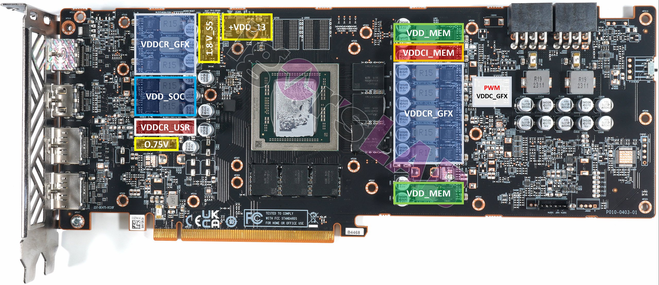
Since questions were asked again and again, which voltages these are in detail, I’ll explain the more unknown voltages today. The acronym “VDD” stands for “Voltage Drain-Drain”, which comes from the MOSFET terminology, and it serves as a term for the supply voltage. This term will come up again and again now, so I’d better explain it up front. And now let’s briefly go into the details of the “Magic Five”.
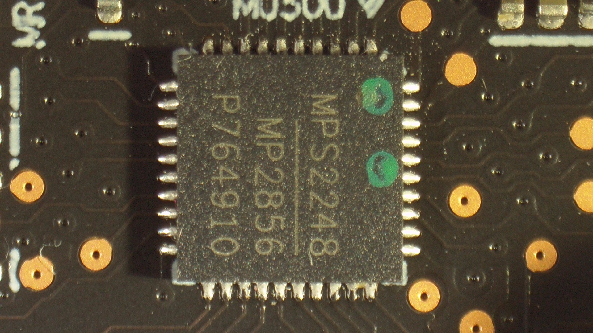
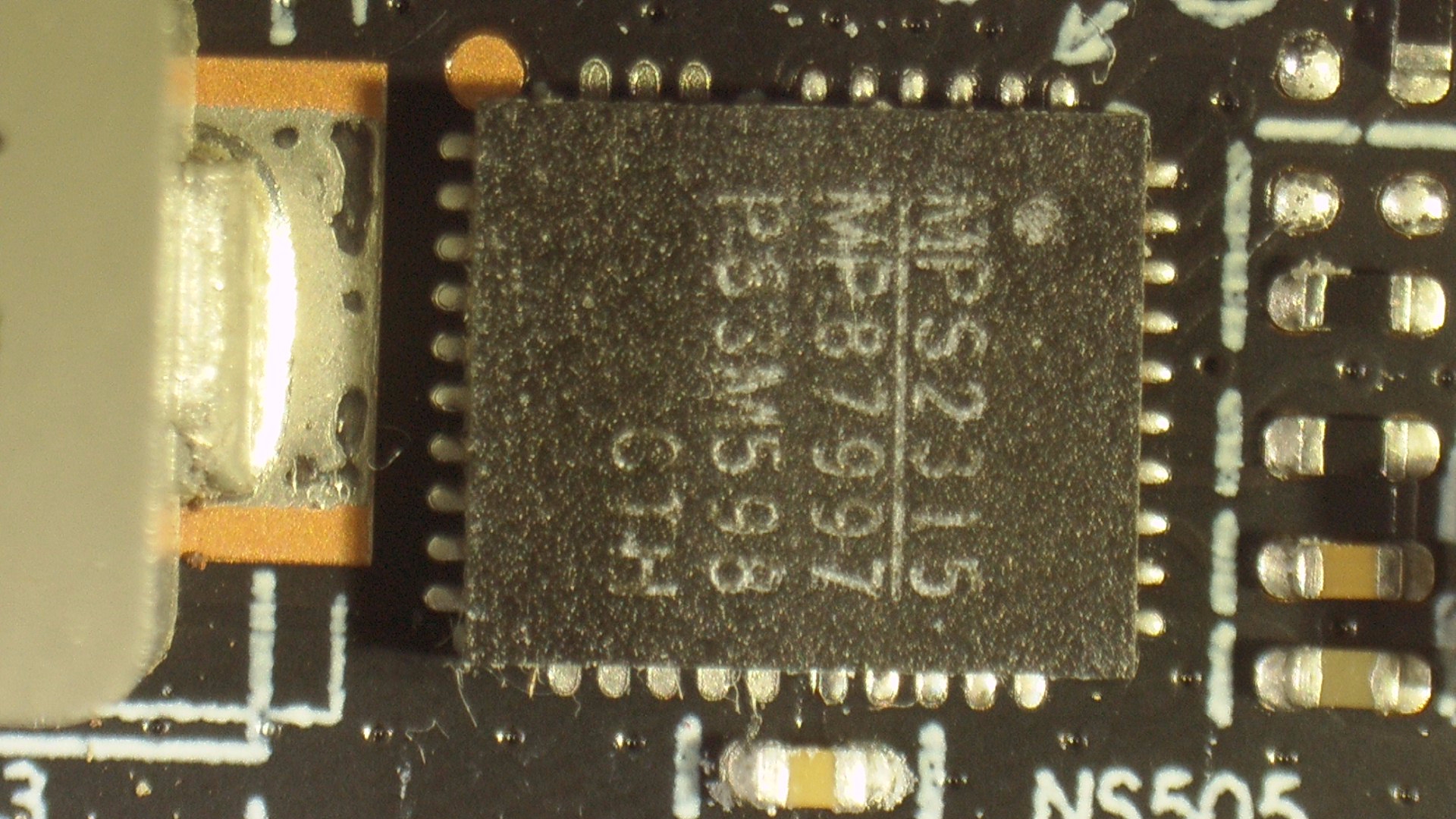
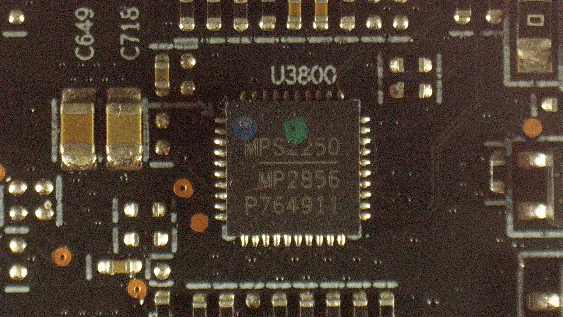
The power supply, of course, relies on VDDCR_GFX (i.e. the equivalent of NVIDIA’s NVVDD) as the largest item for the GPU. Sapphire uses eight phases here, each driving a single SPS (voltage regulator). The board would even give a maximum of 9 phases, but they go with a 4 4 phase controller from Monolith with the MP2856 at 8 phases (the MP2857 with 8 4 for 9 phases would then be for 9 phases) with AMD’s SVI2 interface. It is a digital, multi-phase, dual-rail controller that primarily provides power to PWM VID cores and is also compatible with the AVSBus interface. In addition, it can work with Monolith’s Intelli-Phase products to implement the multiphase voltage regulator (VR) solution with a minimum of external components. Therefore, they use the MP87997 as a PLC from the same manufacturer as Smart Power Stages (PLC).
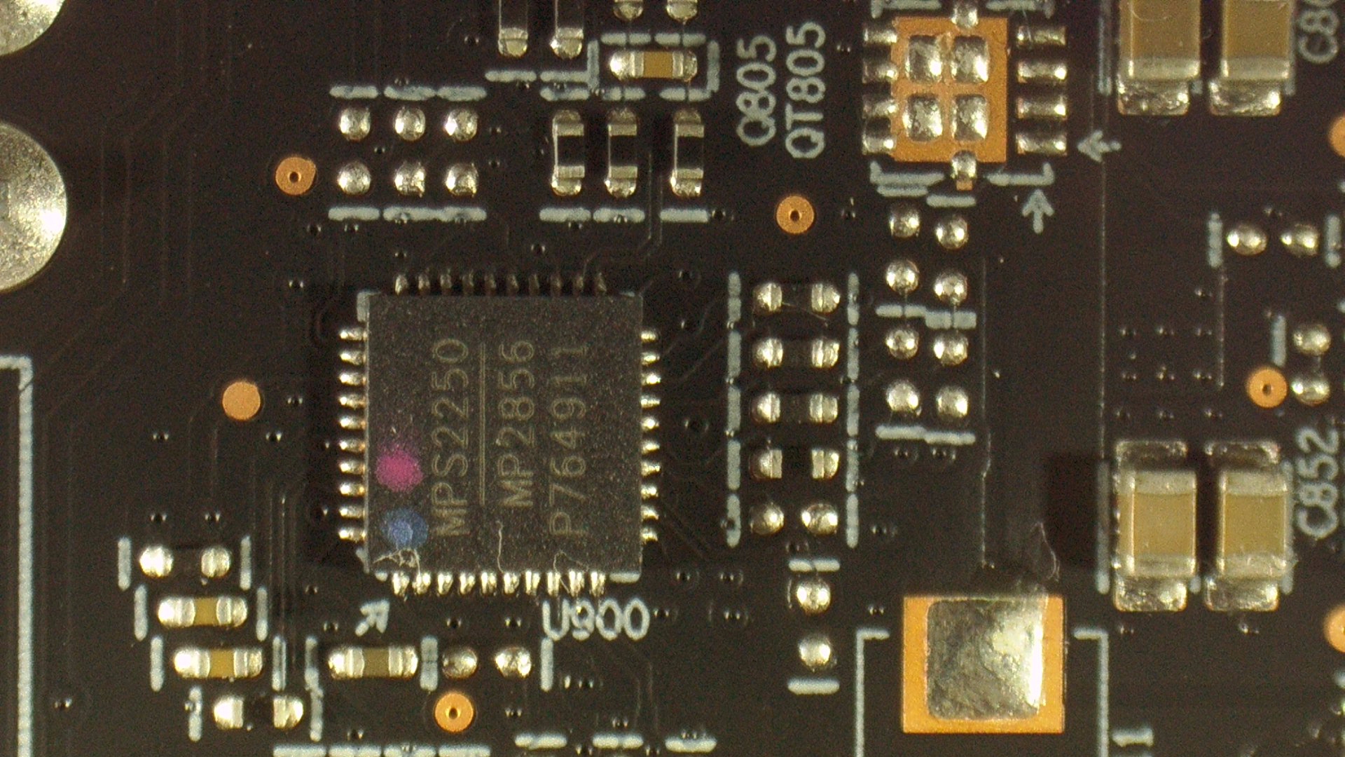
Another PWM controller of the same type controls two phases for VDD_SOC and one for VDD_USR. VDD_SOC writes the supply voltage level that drives the System-on-Chip. This voltage level is important to the operation of the SoC and must be precisely specified and regulated to ensure that the chip functions properly. Even more mysterious, however, is VDD_USR. The USR stands for Ultra-Short Reach and it should actually be called USR_PHY. Because this is about a voltage for the inter-die communication and PHY stands for the physical layer of a connection protocol. Or in short, the MCM components of the chiplet design also want and have to exchange data with each other.
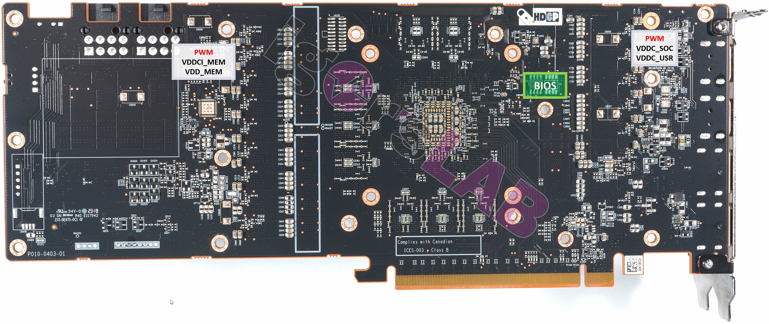
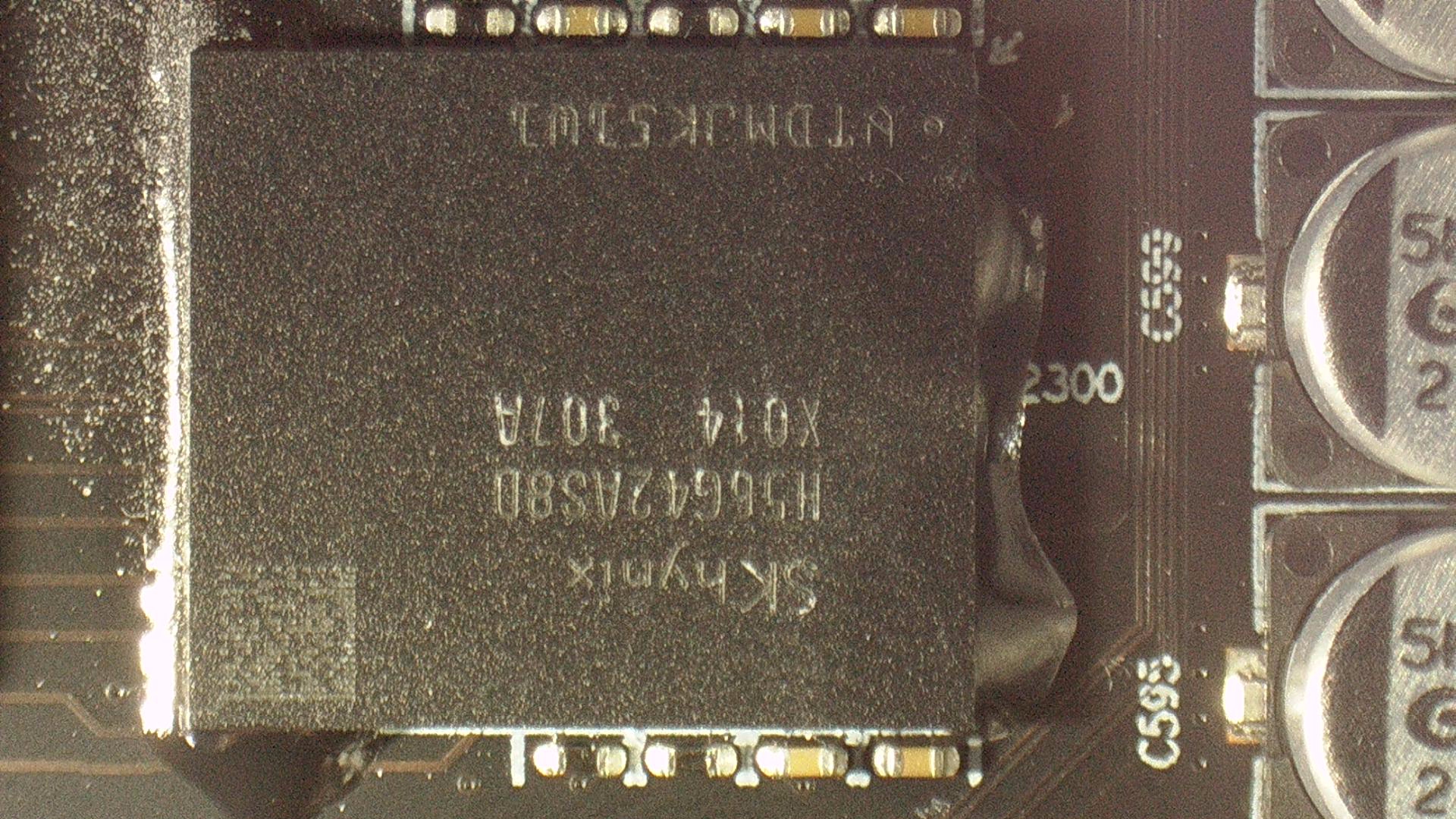
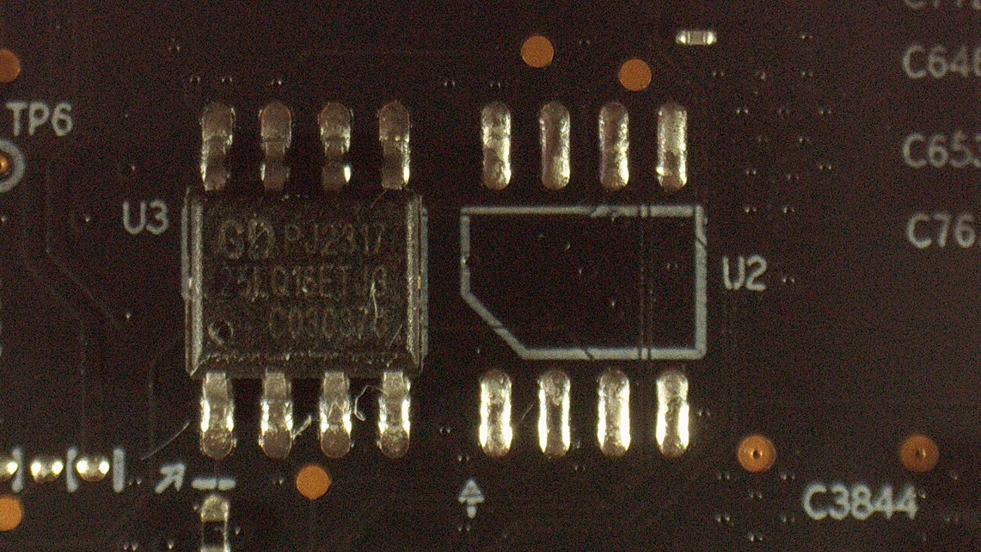
The PWM controllers for the voltage supply of the memory VDD_MEM and VDDCI_MEM are located near the back. Here (as with VDD_USR and VDD_SOC) a cheaper MP2853 from Monolith would have been enough, but you put the big controller on it. Waste of money, but at least available. VDDCI_MEM isn’t a big item performance-wise, but it’s enormously important. It serves the GPU-internal level transition between the GPU and the memory signal, something like the voltage between the memory and the GPU core on the I/O bus.
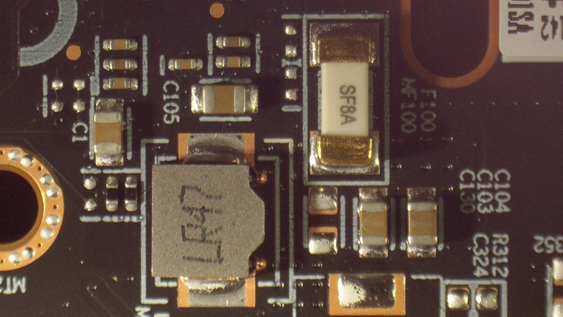
In addition, one generates other extra-low voltages (see front panel schematic). Most of these very similar voltage converters are located on the front side of the board. There is also a 1.8V source (TTL, GPU GPIO), VDD_13 (Aux) and an ultra-low dropout chip generates the very low voltage for the PLL area (VPP). All power stages used, including those for the memory, are also Monolith products. The MP87997 is a very high performance monolithic half bridge and the integration of drivers and MOSFETs (DrMOS) results in high efficiency due to optimal dead time and parasitic inductance reduction. This small, 5 mm x 6 mm LGA device is a perfect fit for the MP2856.


- 1 - Introduction, technical data and technology
- 2 - Test setup and methods
- 3 - Teardown: PCB and components
- 4 - Teardown: Cooler and material analysis
- 5 - Gaming-Performance Full-HD (1920 x 1080)
- 6 - Gaming Performance WQHD (2560 x 1440)
- 7 - Details: Power consumption and balancing
- 8 - Transients and PSU recommendation
- 9 - Temperatures, clock rate and thermal imaging
- 10 - Fan curves and noise
- 11 - Summary and conclusion


288 Antworten
Kommentar
Lade neue Kommentare
Mitglied
Mitglied
Urgestein
1
Veteran
Veteran
Urgestein
Veteran
Mitglied
Mitglied
Urgestein
Urgestein
Mitglied
Mitglied
Urgestein
Mitglied
Urgestein
Urgestein
Urgestein
Alle Kommentare lesen unter igor´sLAB Community →