


Teardown: PCB layout and components
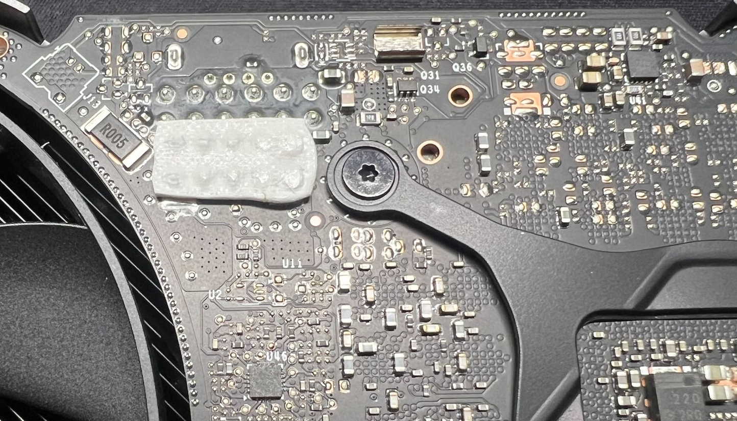
Let’s start with the circuit board first. NVVDD is still the most important voltage, resulting in a voltage converter design with a total of 6 true phases and the resulting 6 control loops for NVVDD alone. Compared to the RTX 4070 Ti, you save a lot, which is just about acceptable in view of the significantly lower TDP. Eight phases would have been preferable to me and certainly more sensible in view of possible hotspots and higher efficiency. But it should also be about the price and so there must be a compromise.
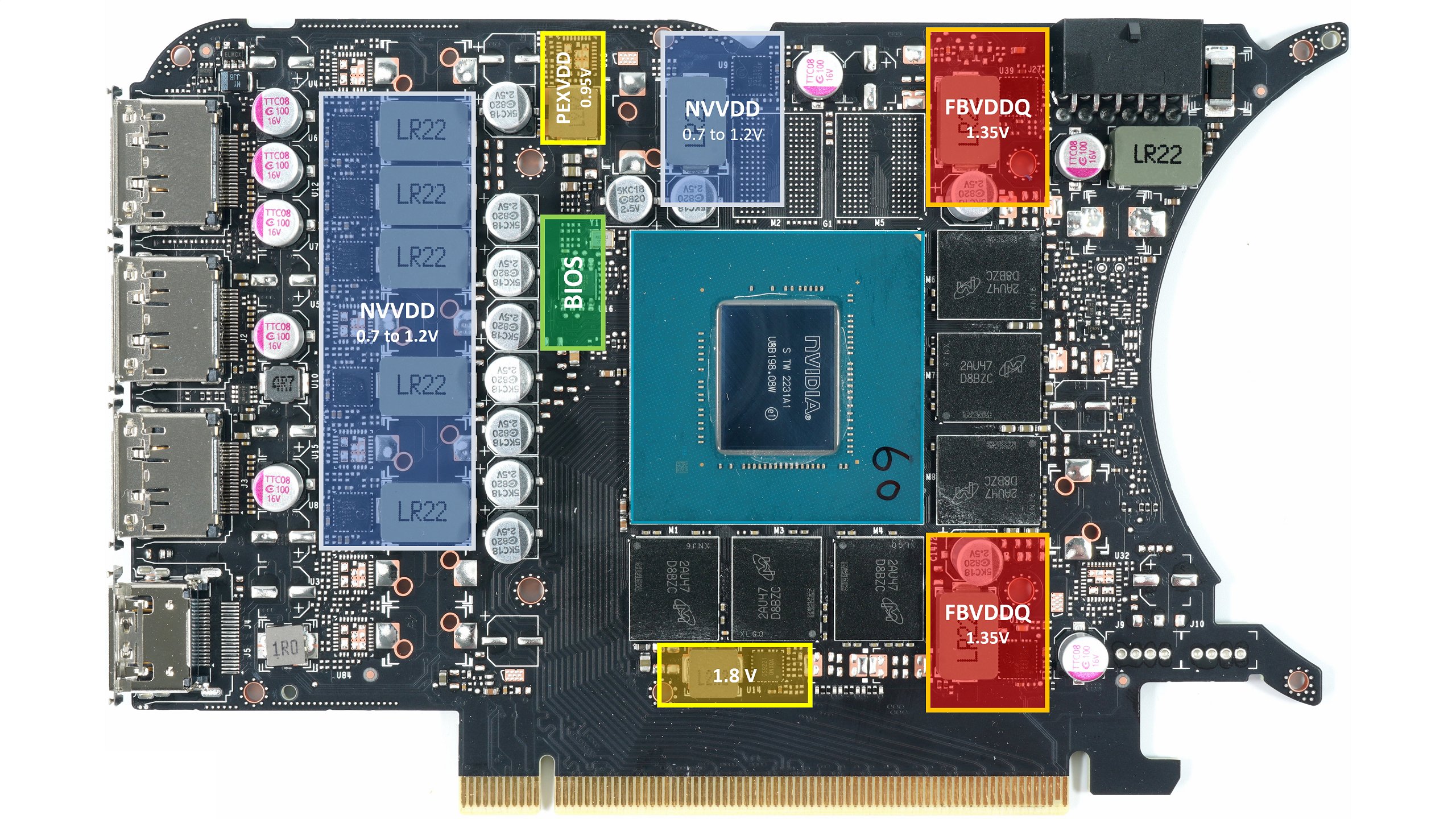
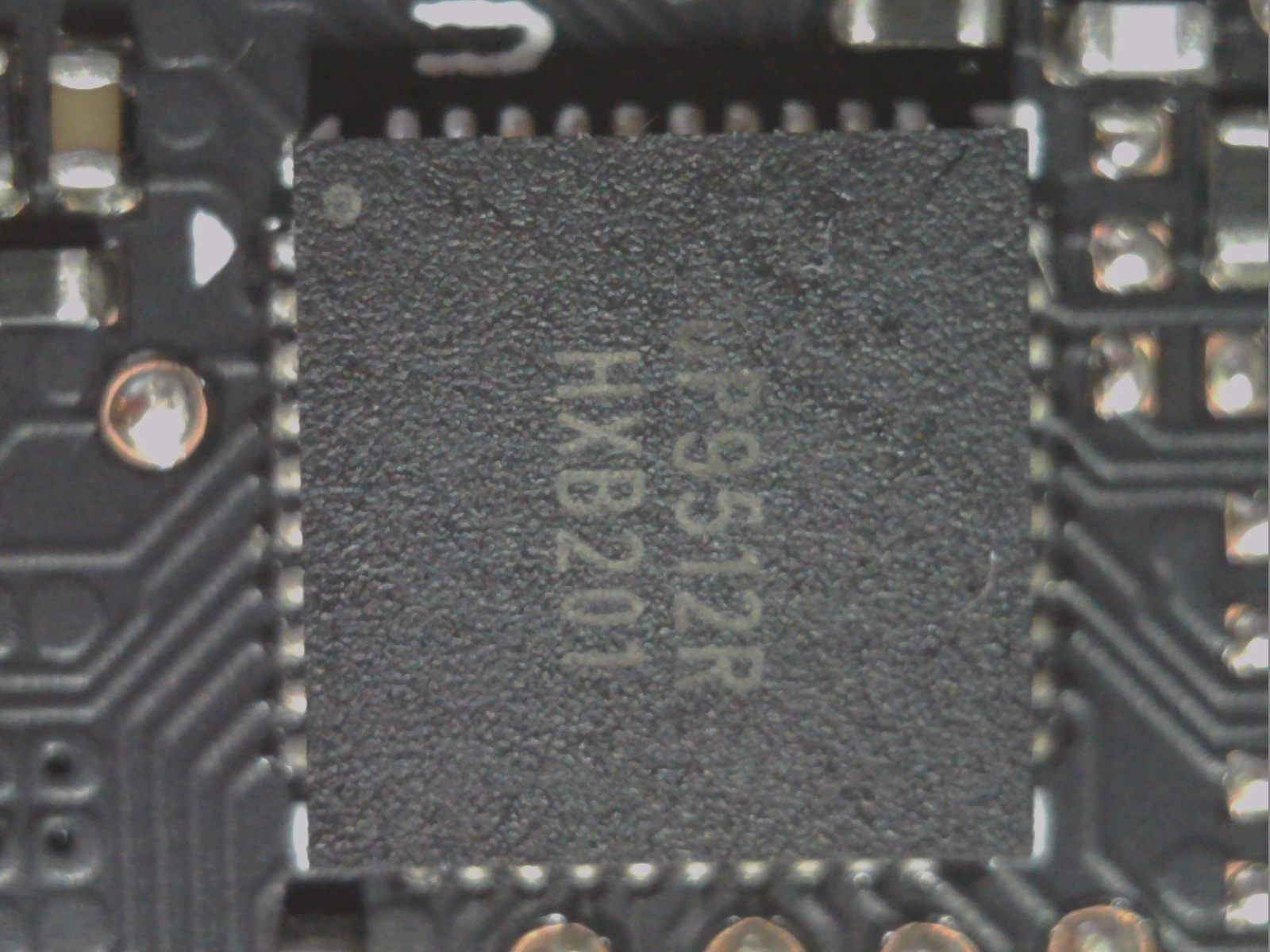
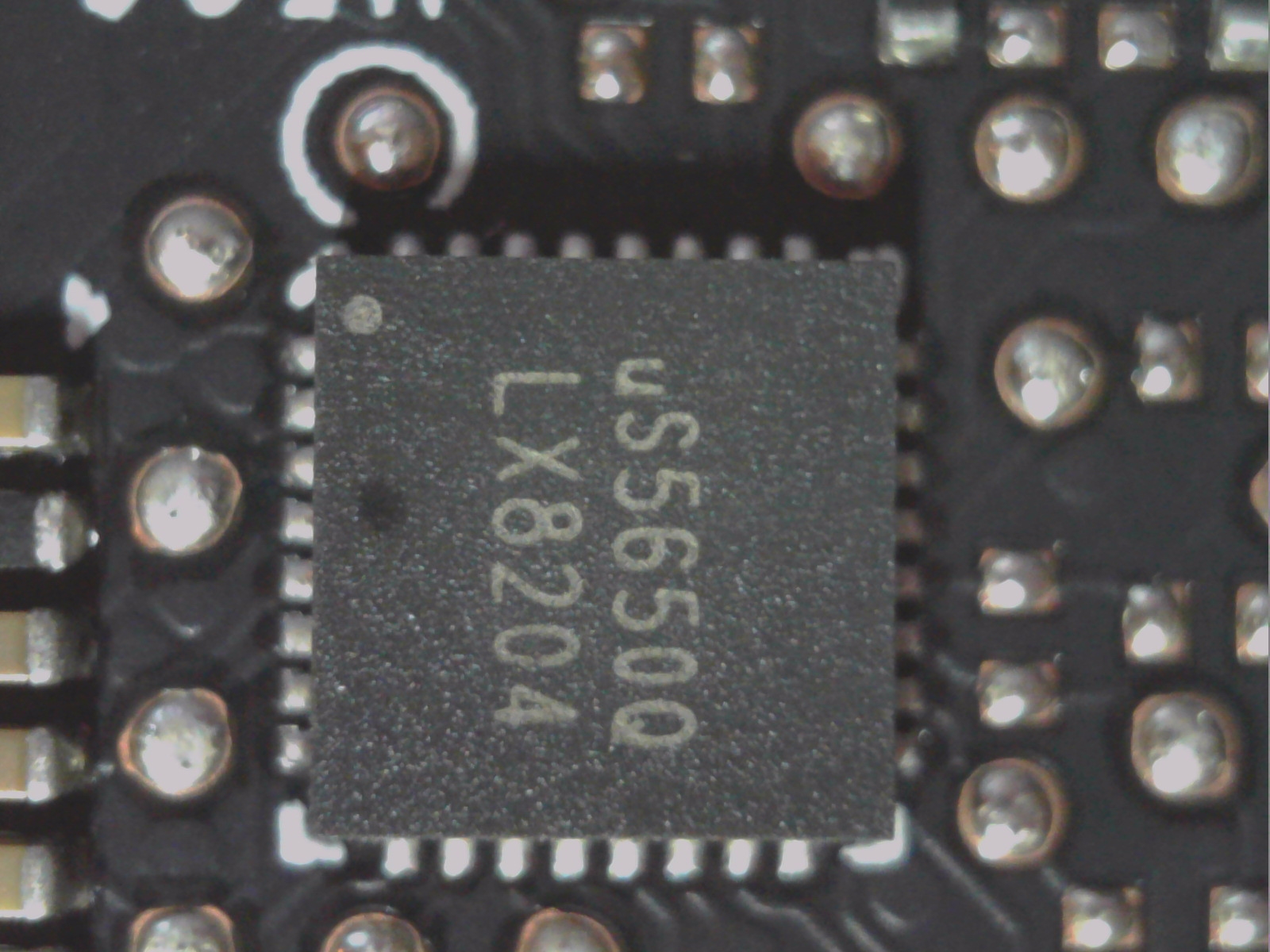
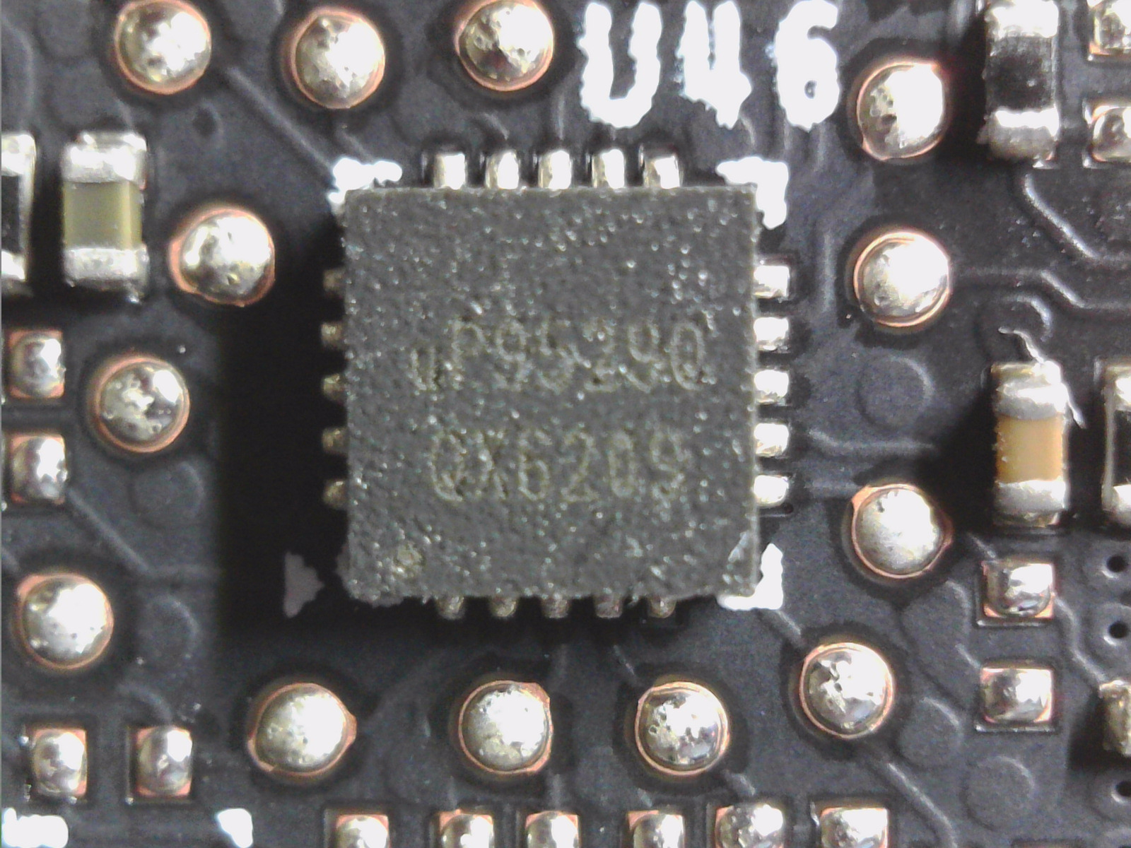
It all looks a bit lean, but we’ll have to get through that for now. One also uses separate PWM controllers for NVVDD (GPU core) and FBVDDQ (memory) again, because the top models among the PWM controllers are unfortunately much too expensive. And therefore it must again the good and well-known uP9512R from UPI Semi fix, which can generate only 8 phases and is significantly cheaper, but which is quite sufficient. A second PWM controller in the form of the small uP9529 then controls the two phases for the memory. By the way, both controllers are located on the back of the board. Directly in between is a uPI uS5650Q for monitoring the four 12V rails (3x Aux and 1x PEG).
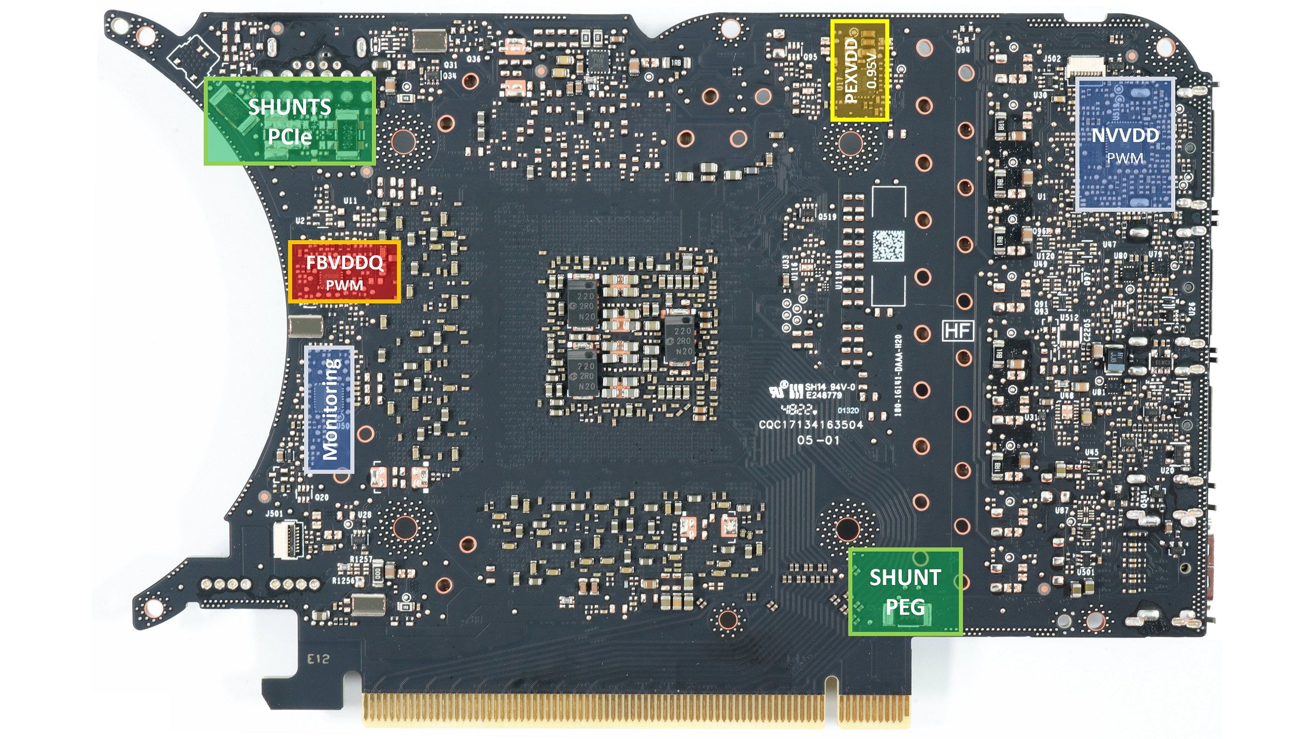
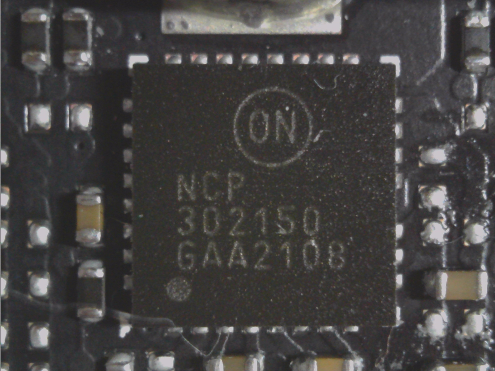
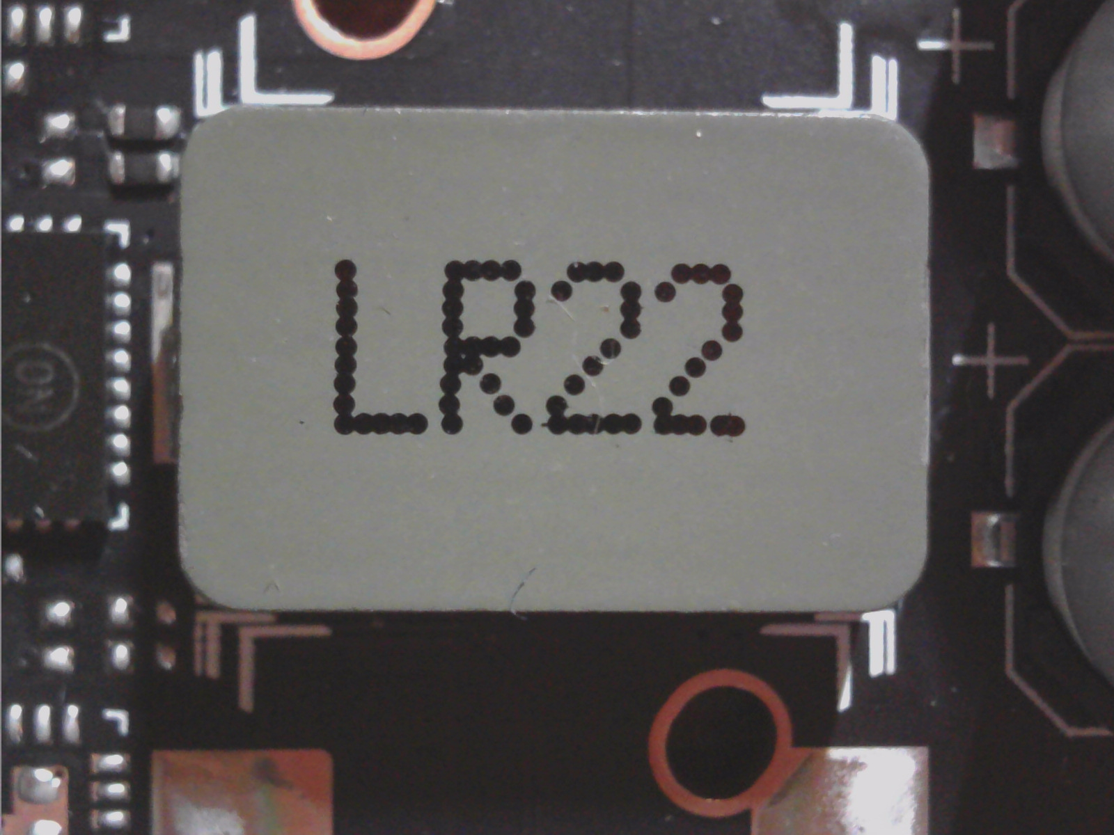
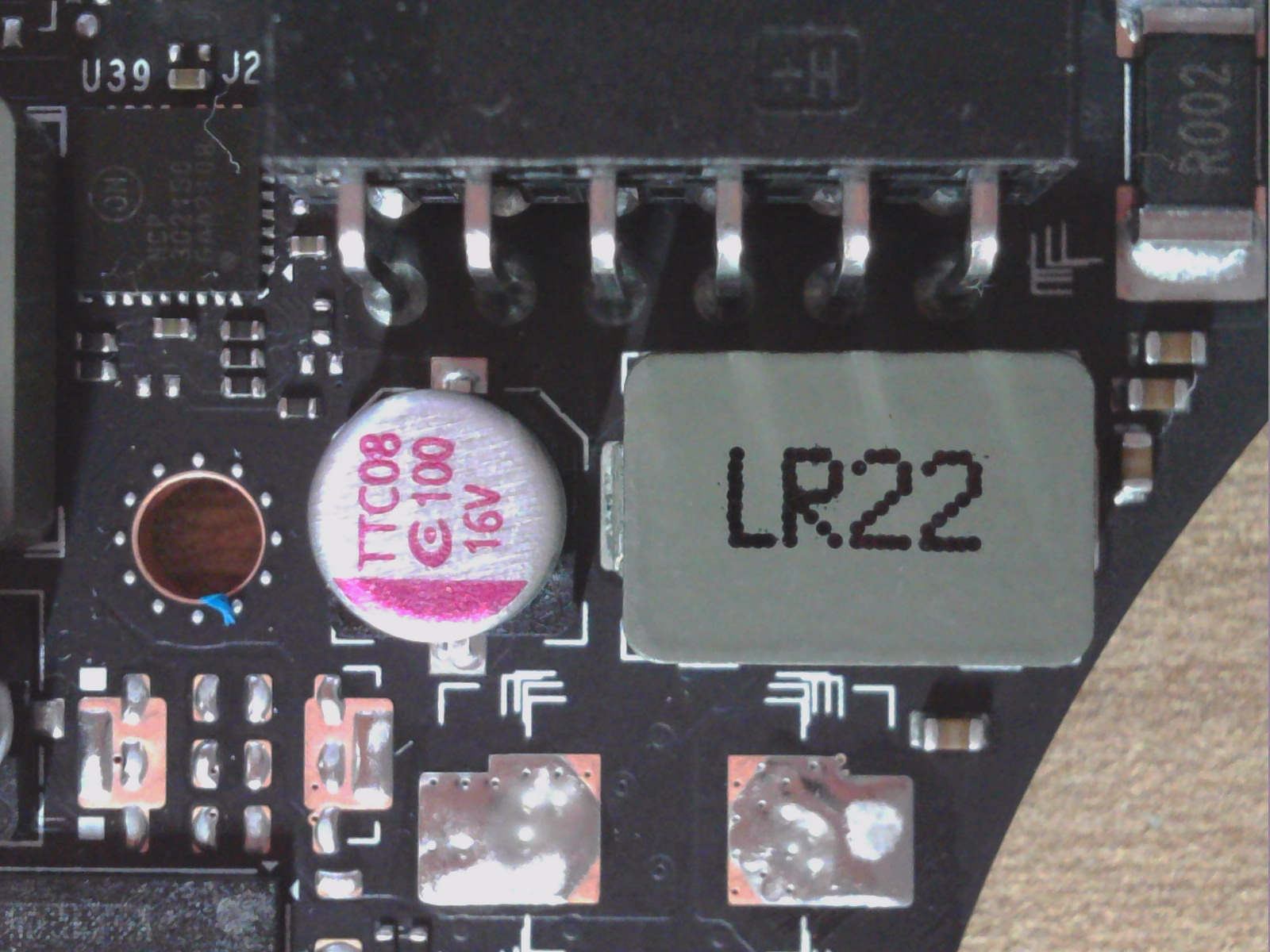
All the DrMOS used, including those for the memory, are rather inexpensive products from OnSemi. Used in all control loops for NVVDD and FBVDDQ (memory), the 50 A peak current NPC302150 integrates a MOSFET driver, high-side MOSFET and low-side MOSFET in a single package. This chip is specifically designed for high current applications such as DC-DC buck power conversion applications. This integrated solution reduces the space required on the PCB compared to a solution with discrete components. The coils used for NVVDD and the memory have an inductance of 220 nH, and the capacitors are in cup form, which is cheaper.
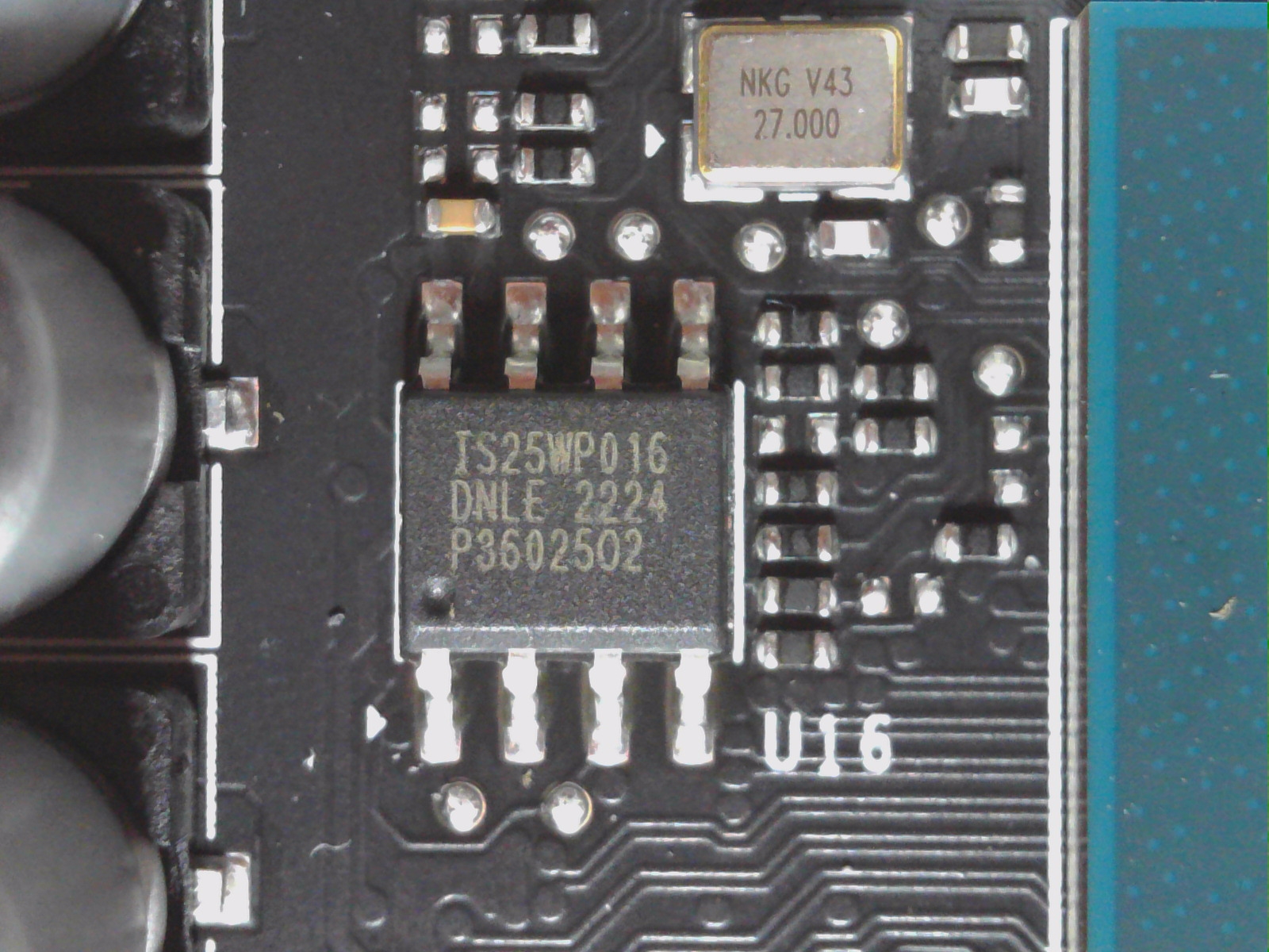
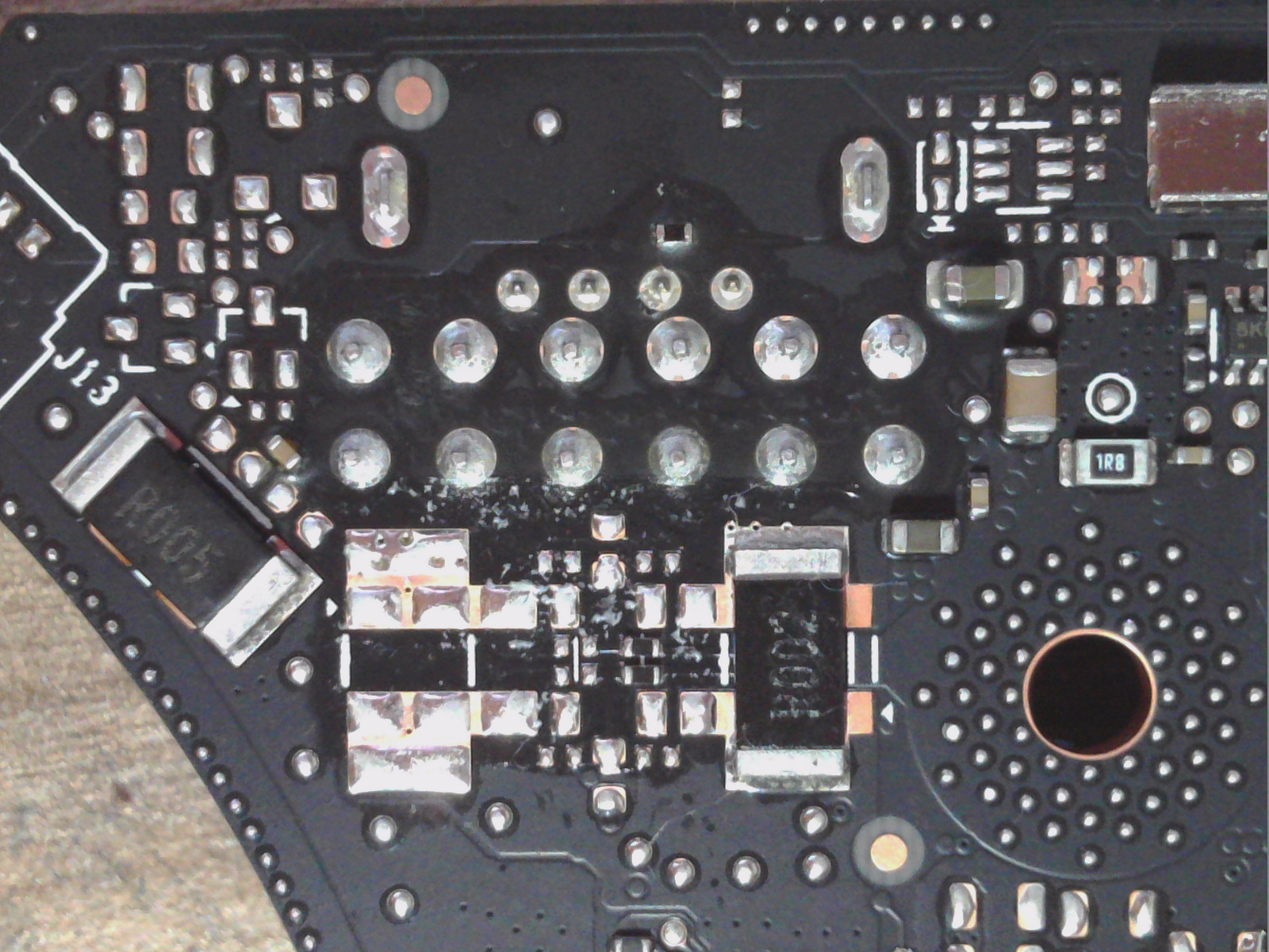
The 12V rails on the 12+4 12VHPWR connector are combined into a single rail directly after the socket, another is connected to the PEG, and is only slightly used for NVVDD. The BIOS is in the usual place and the generation of the remaining extra-low voltages is also as usual. So there are no more special features.

Teardown: The cooler
The magnetic back cover is naturally set and disassembly has rarely been easier. Two lugs to hook onto the end of the card and a small snap mechanism on the slot panel are all you need to use. The rest just clicks.
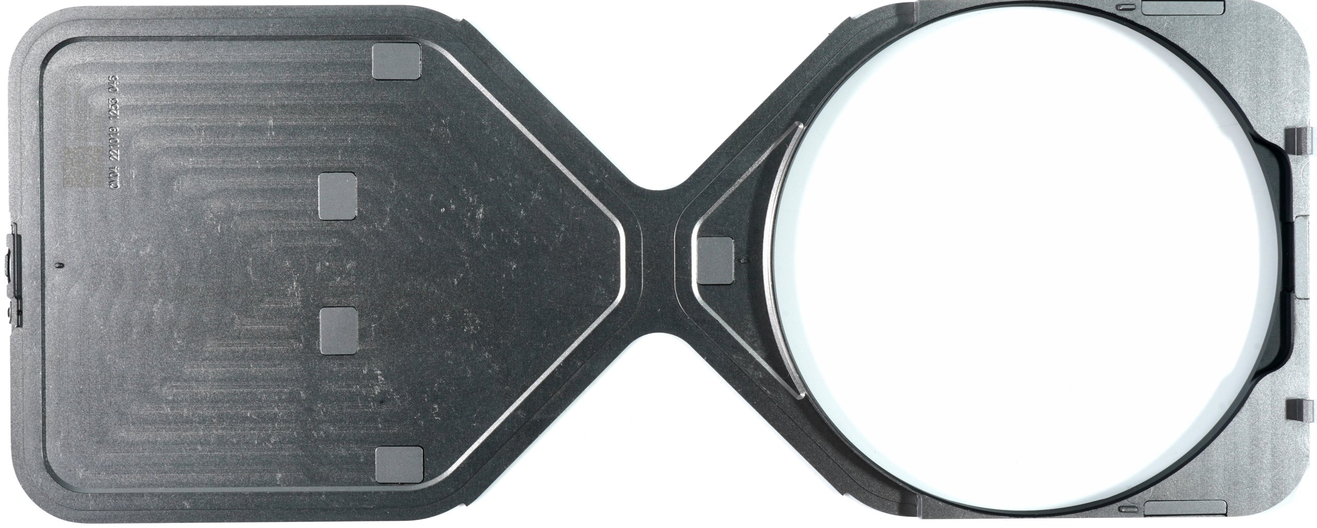
The actual, firmly screwed backplate, which is also used for cooling, is then located directly underneath. If you remove the screws, the circuit board is exposed. And if you read my articles carefully, you won’t be surprised about the positioning of the pad at the bottom left of the rounding, because…
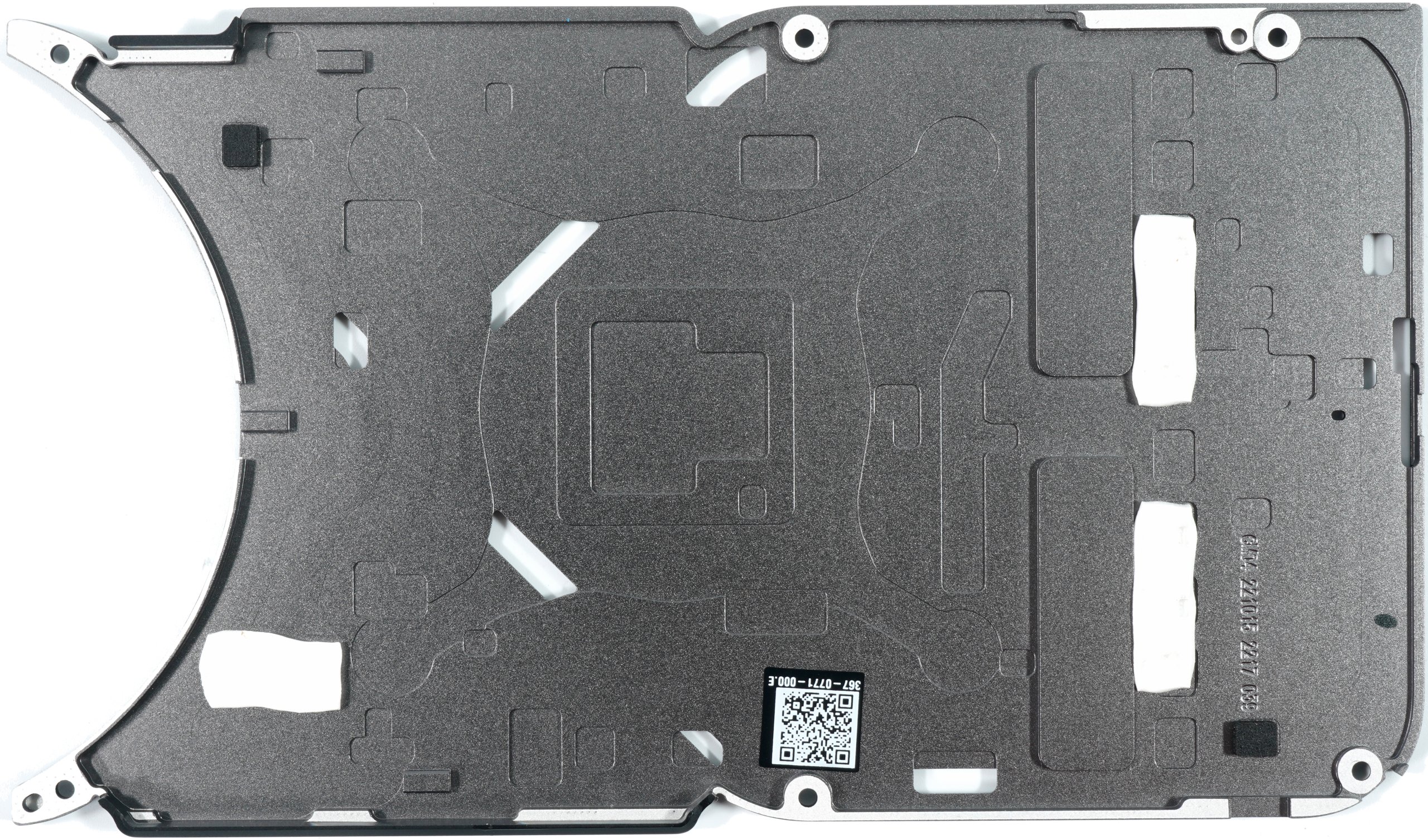
…it is my pad mod for the 12VHPWR connection, which I had already thematized and also implemented with the RTX 4090! And NVIDIA has even gone further and placed the shunt (as recommended) on the back (see PCB teardown) and cools it (under the pad) at the same time. Commendable, but at these low currents it is completely unnecessary, as we will see. On the RTX 4090 or RTX 4080, something like this would have made much more sense and been more appropriate. But maybe someone can open his new RTX 4090 FE and have a look. In the case of the GeForce RTX 3080 FE, it was also included in the current production… 🙂
The rest, however, is quickly told. A solid copper heatsink is used instead of the usual vapor chamber and a total of four heat pipes.
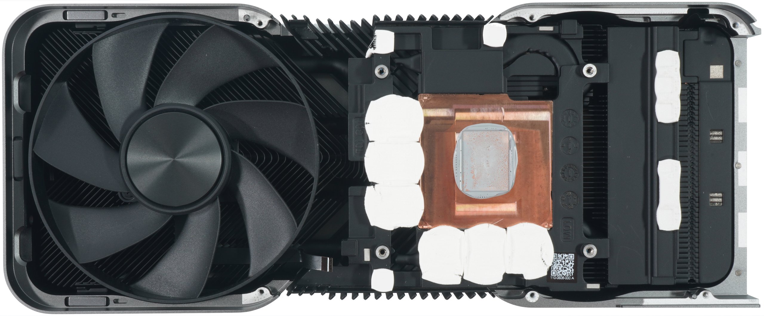
The pads used are in the style of the RTX 3080, ultra-soft and well-deformable, but not top shelf. So cost down here as well. The inverse fan on the back has a rotor diameter of 9 cm and relies on seven rotor blades. The normally oriented fan on the front side has a similar design.

- 1 - Introduction, Specs and Unboxing
- 2 - Test system, equipment and methods
- 3 - Teardown: PCB, components and cooler
- 4 - Gaming Performance Full HD (1920 x 1080)
- 5 - Summe Gaming-Performance WQHD (2560 x 1440)
- 6 - Gaming Performance Ultra HD (3840 x 2160)
- 7 - Gaming Performance DLSS vs. FSR
- 8 - Latency and DLSS 3.0
- 9 - Workstation and rendering
- 10 - Power consumption and PEG loads
- 11 - Transients, cutting and PSU recommendation
- 12 - Clock rate and OC, temperatures and thermal imaging
- 13 - Fan speed and noise level
- 14 - Summary and conclusion


258 Antworten
Kommentar
Lade neue Kommentare
Moderator
1
Urgestein
Neuling
Urgestein
Neuling
1
Veteran
Neuling
Urgestein
Urgestein
Veteran
Mitglied
Mitglied
Veteran
Urgestein
Urgestein
Urgestein
Mitglied
Alle Kommentare lesen unter igor´sLAB Community →