


Teardown: PCB layout and components
I have already discussed the changes in the load change behavior and the power consumption, but more about that later in this review. First, let’s start with the board itself. NVVDD is still the most important voltage, resulting in a voltage converter design with a total of 8 phases and the resulting 16 control loops for NVVDD alone (two in parallel per phase). The GeForce RTX 3090 Ti still relied on 8 phases and a total of 24 voltage converters, so three per phase in parallel, and the RTX 4090 Founders Edition on 10 phases and 20 voltage converters. And then MSI comes with 16 and 8 phases. Thus, you save a bit, but this also seems reasonable in view of the significantly lower TDP.
That one relies on a solid parallel circuit instead of phase doubling makes perfect sense, because with the now also higher switching frequencies the double number of phases would only be a hindrance due to the inertia of the coils and caps. Cheaper cards still rely on simple 8-phase without parallel connection, because the PWM controllers and also the DrMOS cost hard cash. And so MSI probably made a compromise in the end.
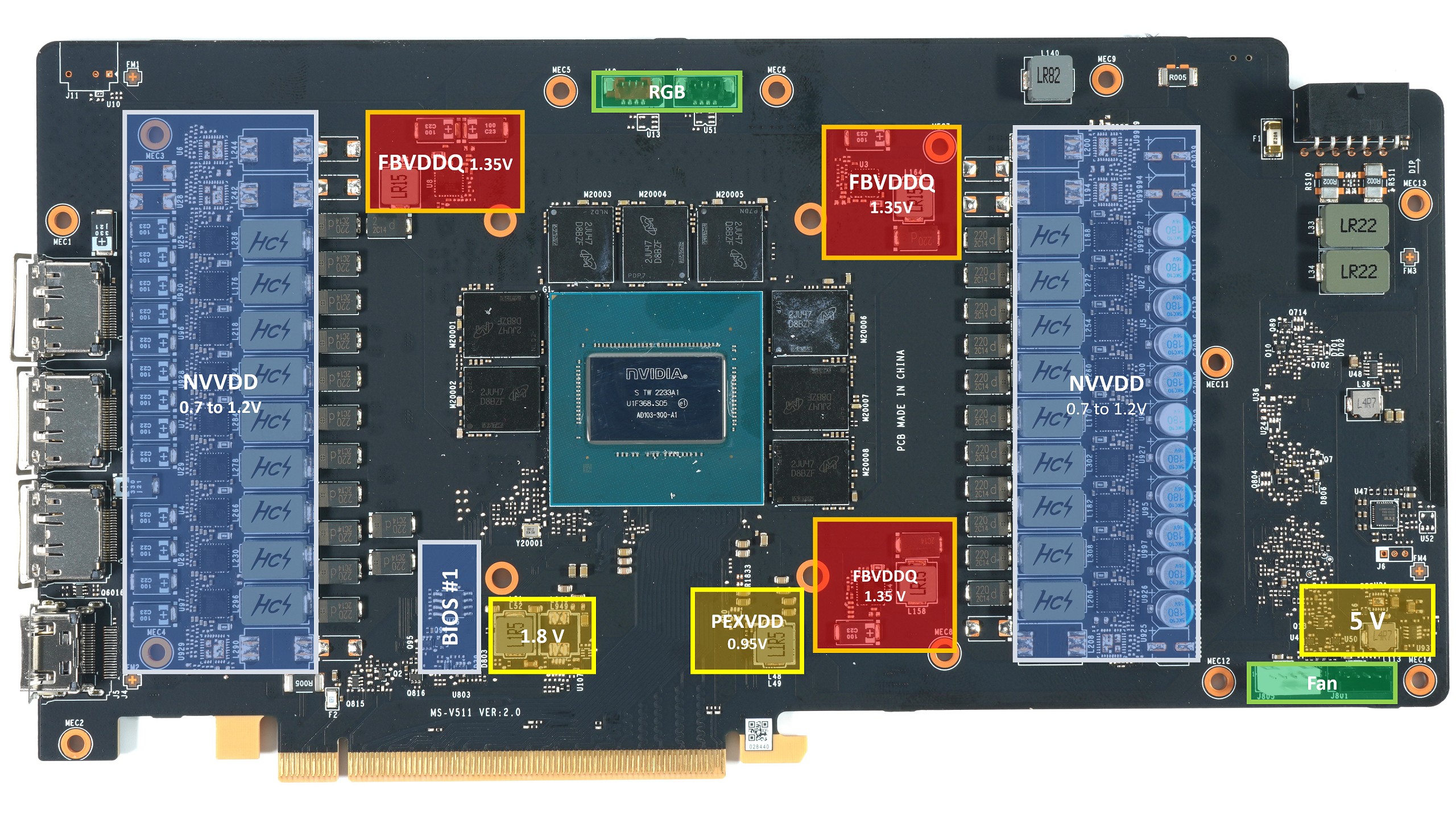
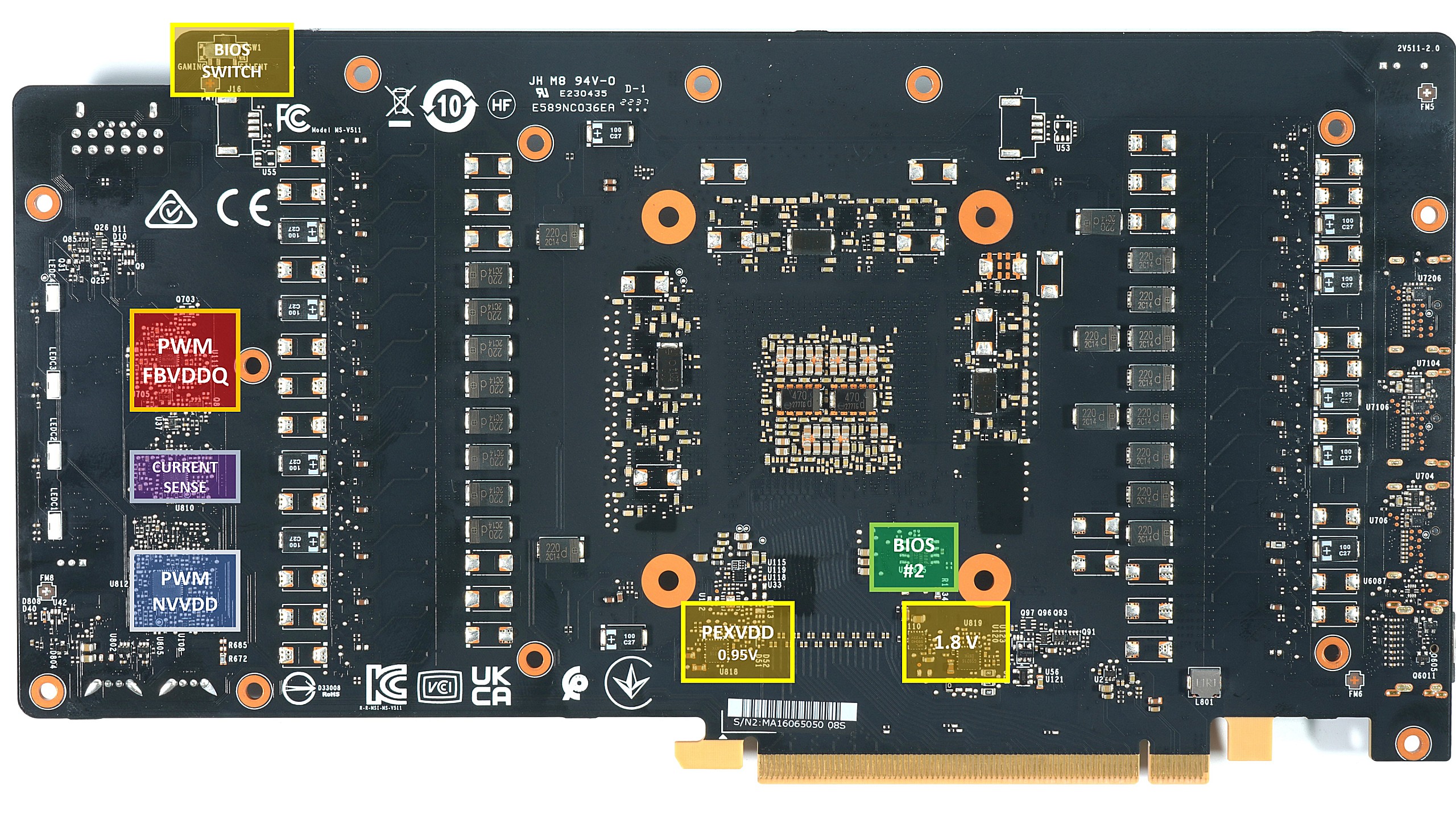
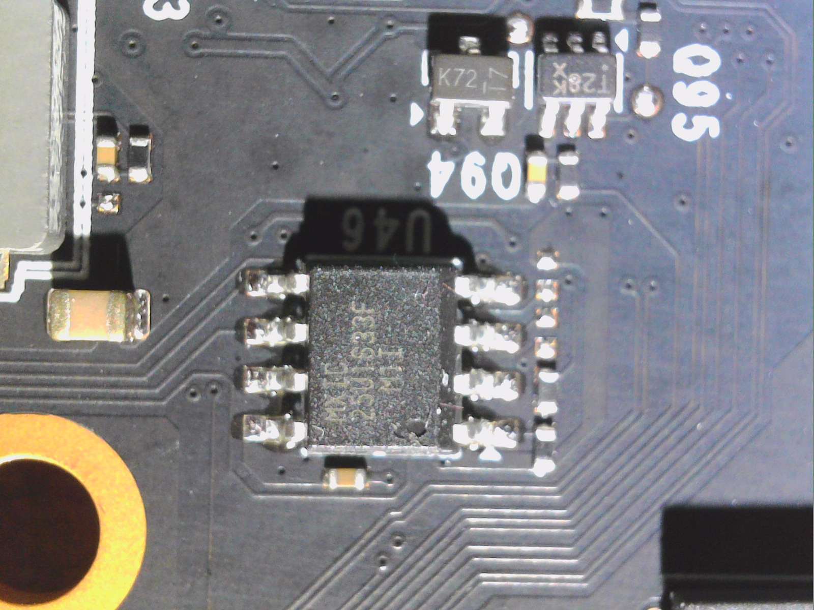
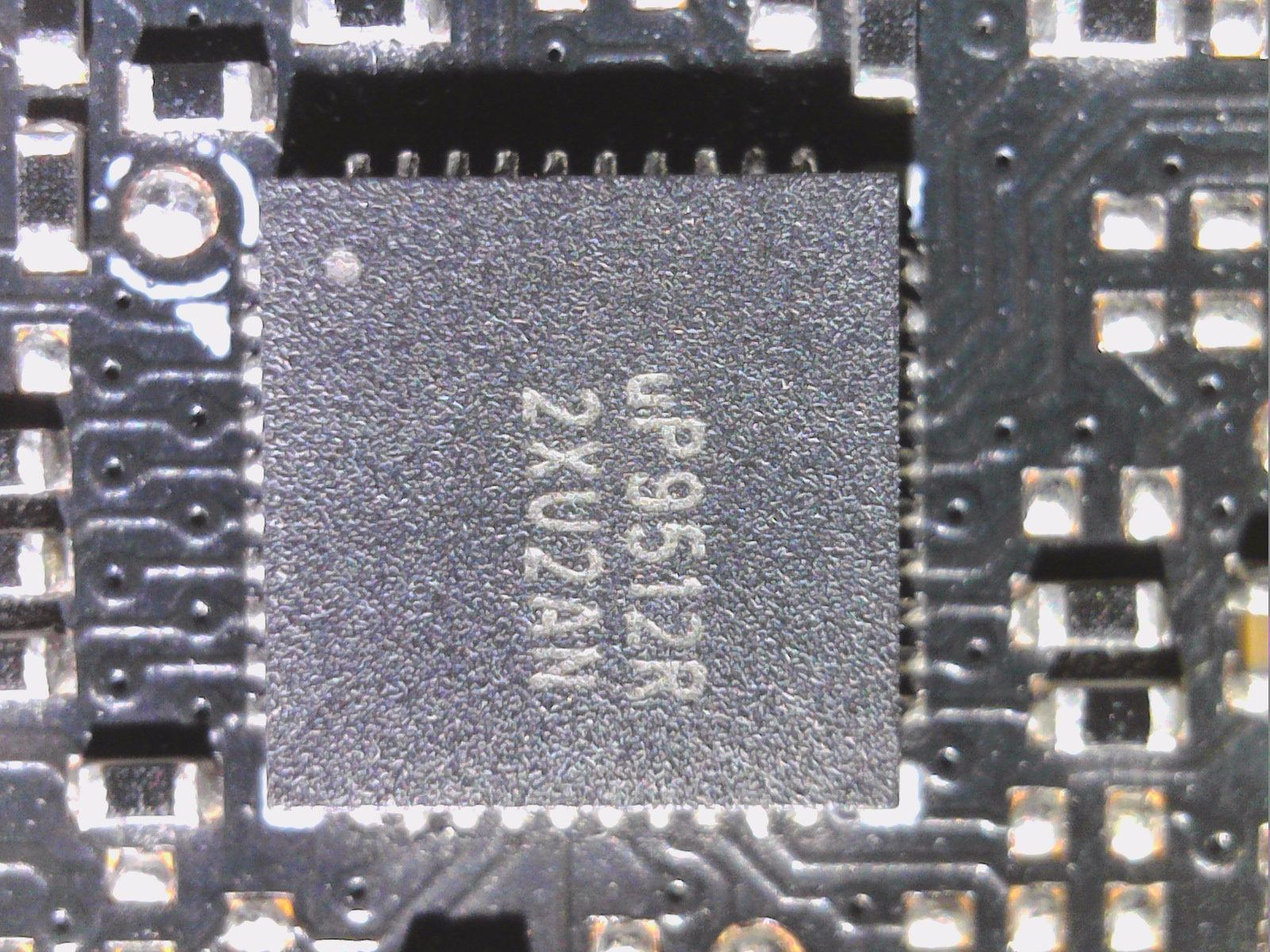
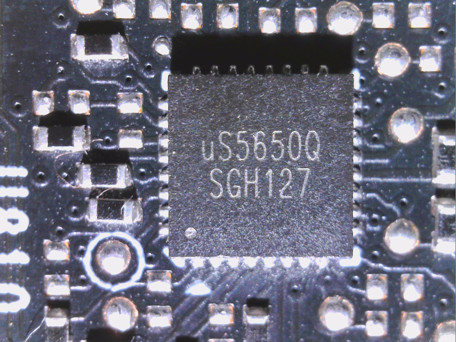
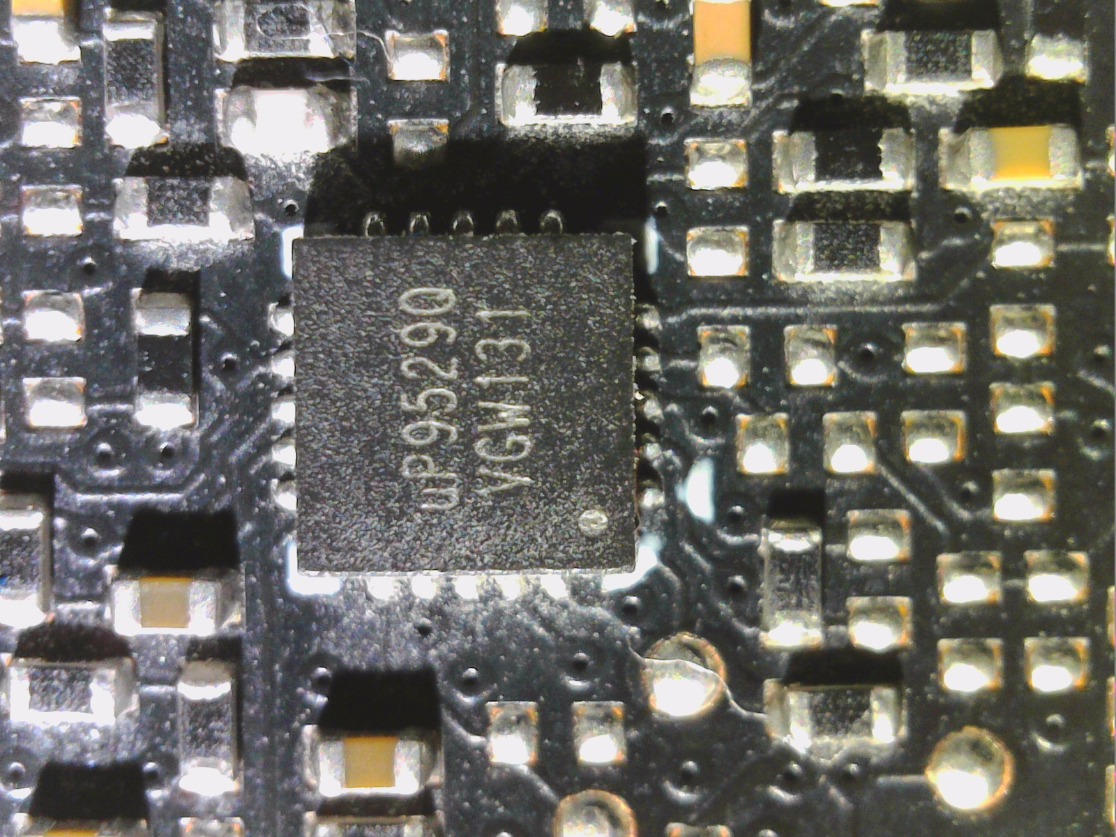
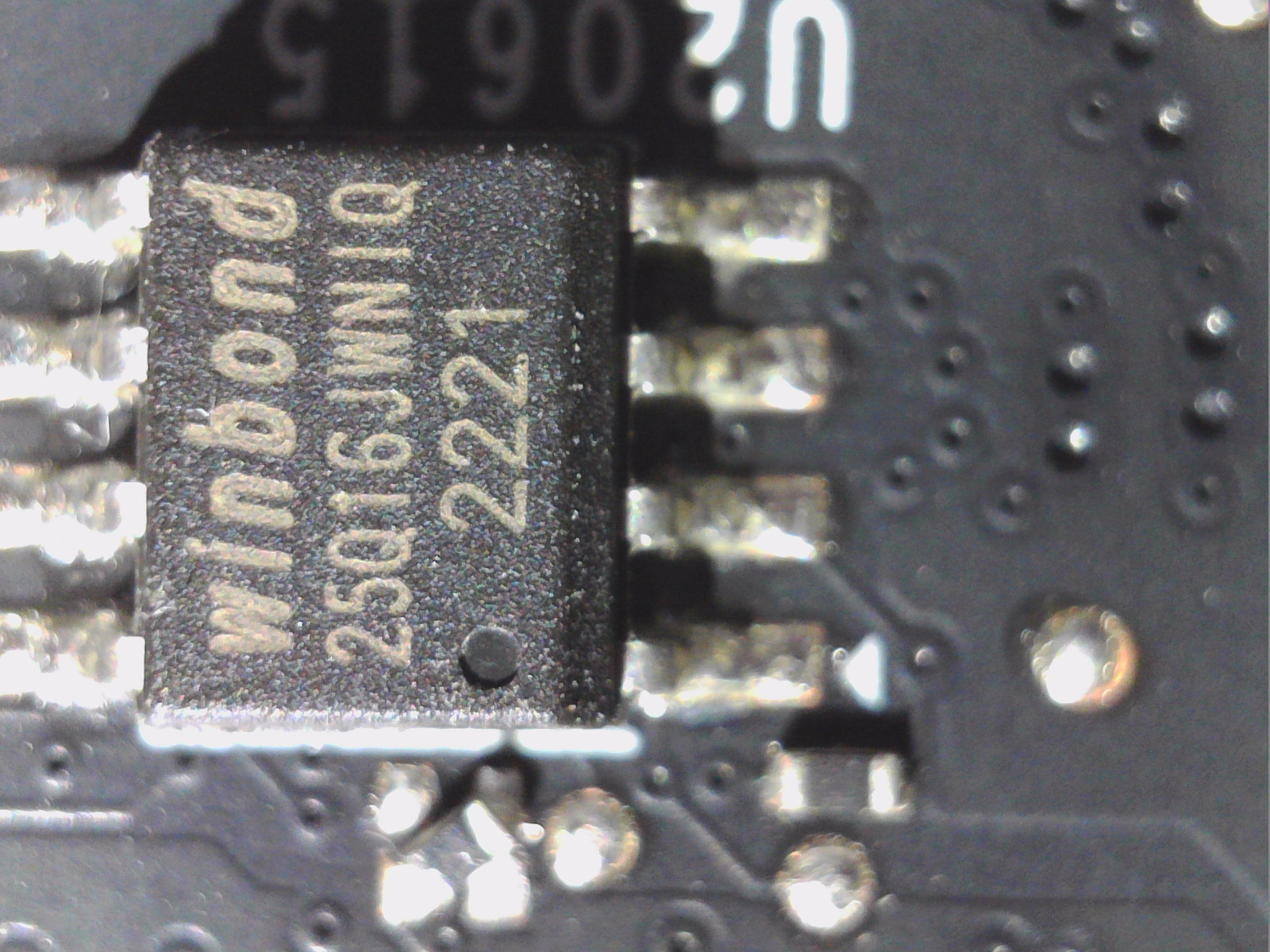
Thus, separate PWM controllers for NVVDD (GPU core) and FBVDDQ (memory) are used again, because the one on the GeForce RTX 4090 MP2891 from Monolith is currently one of the top models among PWM controllers and unfortunately also much too expensive. Therefore, the good and well-known uP9512R from UPI Semi, which can only generate 8 phases and is significantly cheaper, has to do it again. A second PWM controller in the form of the small uP9529 then controls the three phases for the memory. By the way, both controllers are located on the back of the board. Directly in between is a uPI uS5650Q for monitoring the four 12V rails (3x Aux and 1x PEG).
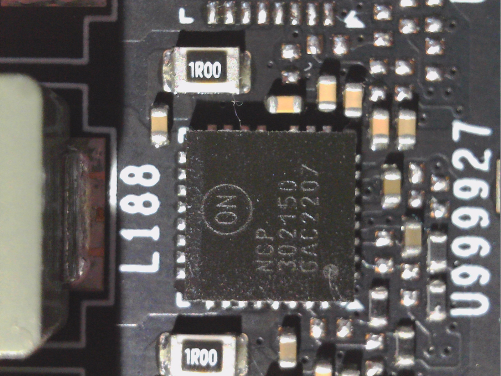
All DrMOS used, including those for the memory, are products of ON Semiconductor. The NCP 302150 is a monolithic half-bridge and integrates a MOSFET driver, high-side MOSFET and low-side MOSFET in a single package. This chip is specifically optimized for high current applications such as DC-DC buck power conversion applications. This integrated solution reduces the space required on the PCB compared to a solution with discrete components.
The coils used for NVVDD have an inductance of 120 mH, those for the memory one of 150 mH. MSI has made an effort to improve the quality, especially in the larger models, but it is still never completely without noise. However, they have found a good compromise here, because the card is still relatively quiet compared to simpler solutions.
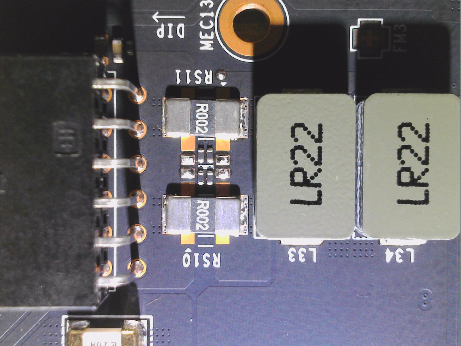
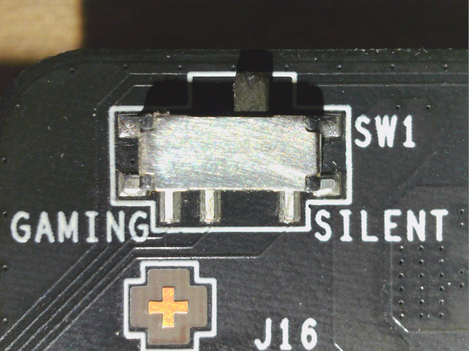
The two 12V rails on the 12+4 12VHPWR connector are combined to one rail after the two shunts (one per rail), another one is connected to the PEG but not used for NVVDD. The dual BIOS is in the usual place and the generation of the remaining extra-low voltages is also as usual. So there are no more special features. The BIOS switch is labeled and set to Silent ex-factory.

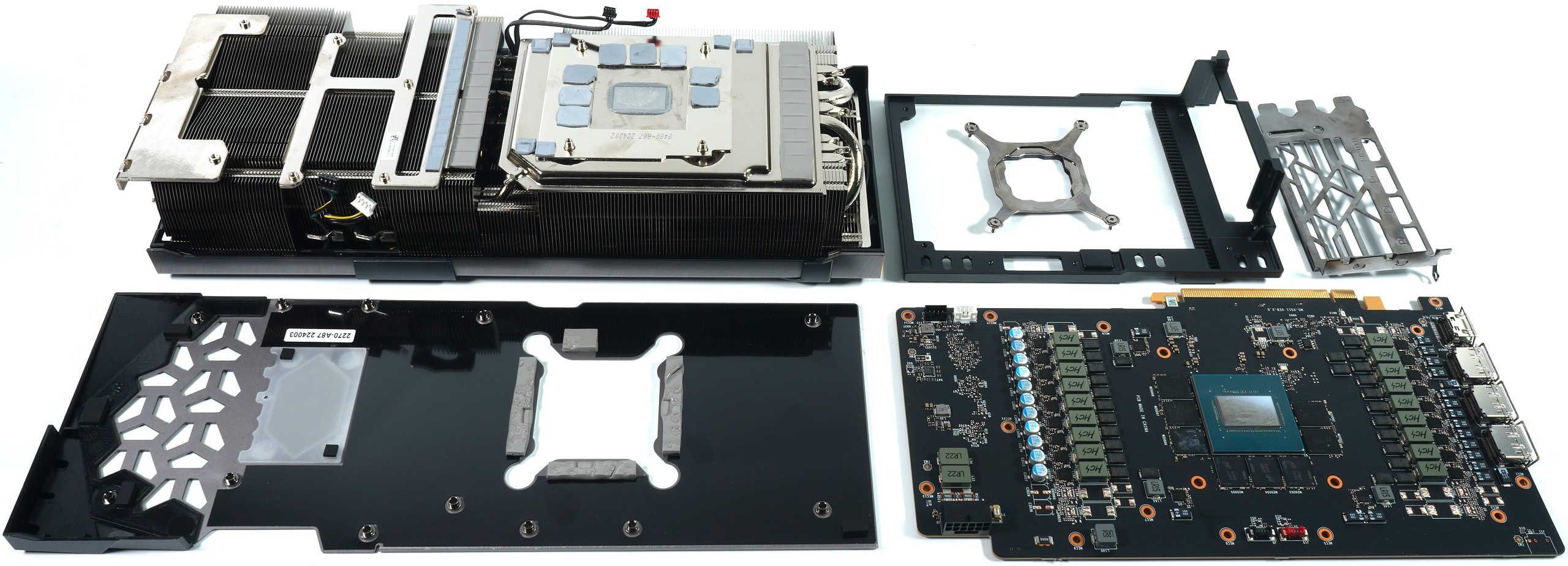
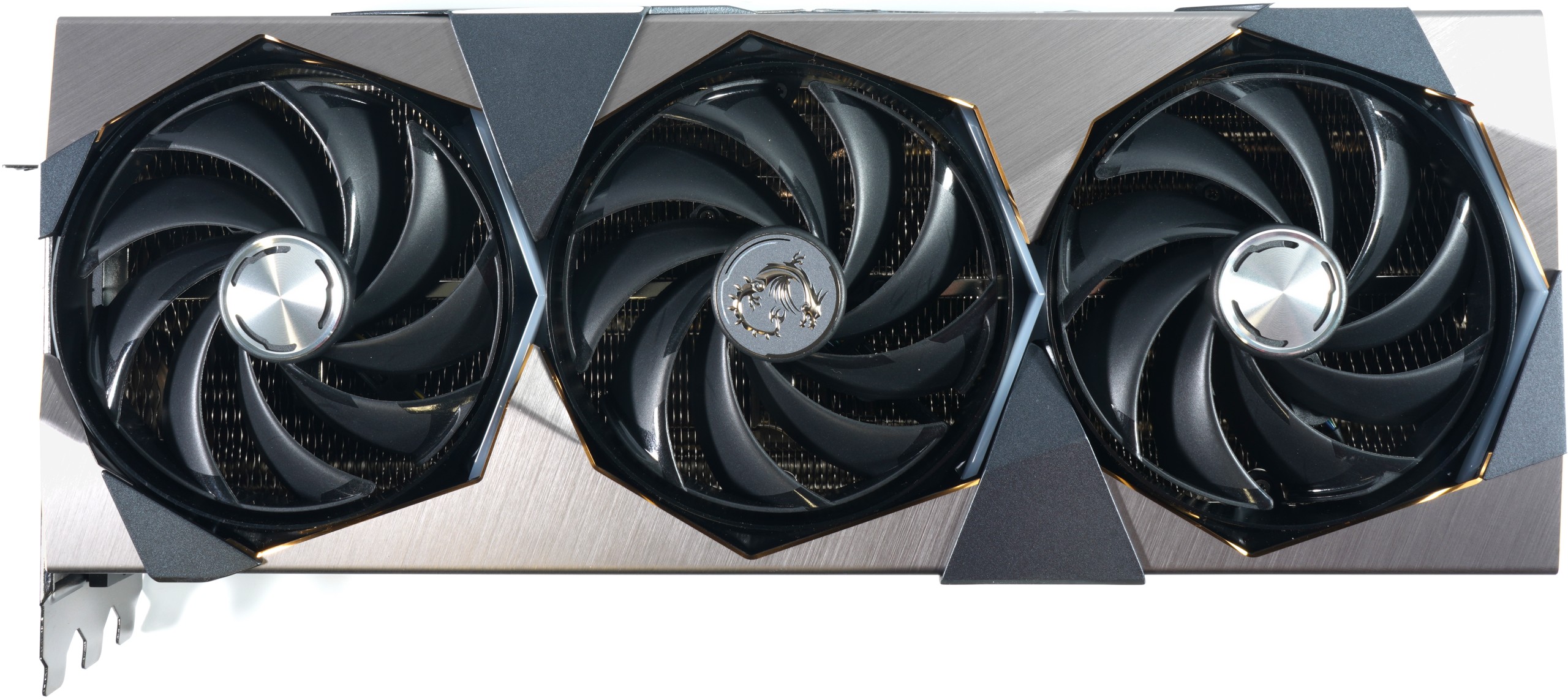
Teardown: The cooler
The actual heatsink cools the GPU and RAM modules via a huge vapor chamber, and the rest is done via the thermally connected massive support structure, which also cools the rear voltage converters. The front area relies on a cooling frame as an attachment (see above), which also stabilizes the slot panel. With two 8 mm heat pipes and five 6 mm heat pipes made of nickel-plated copper composite, the waste heat from the vapor chamber is distributed via the lamella cooler.
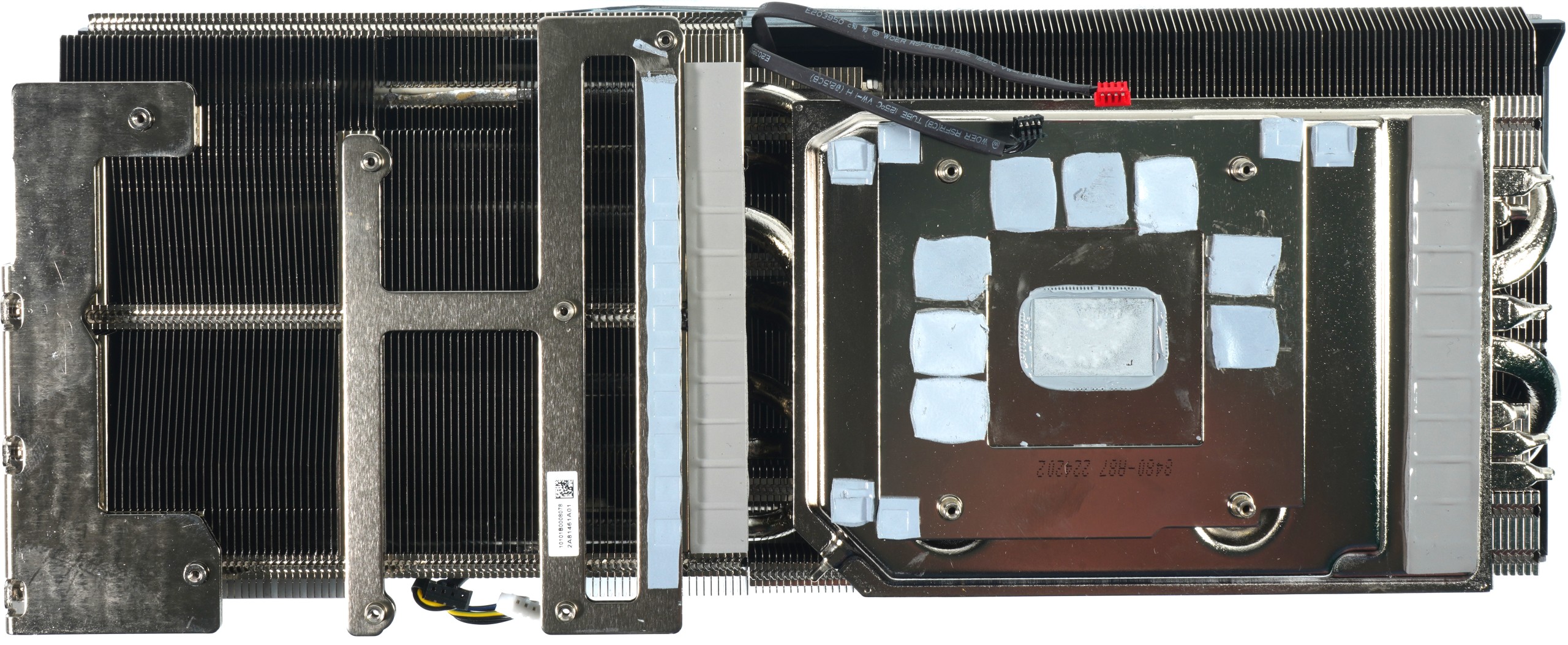
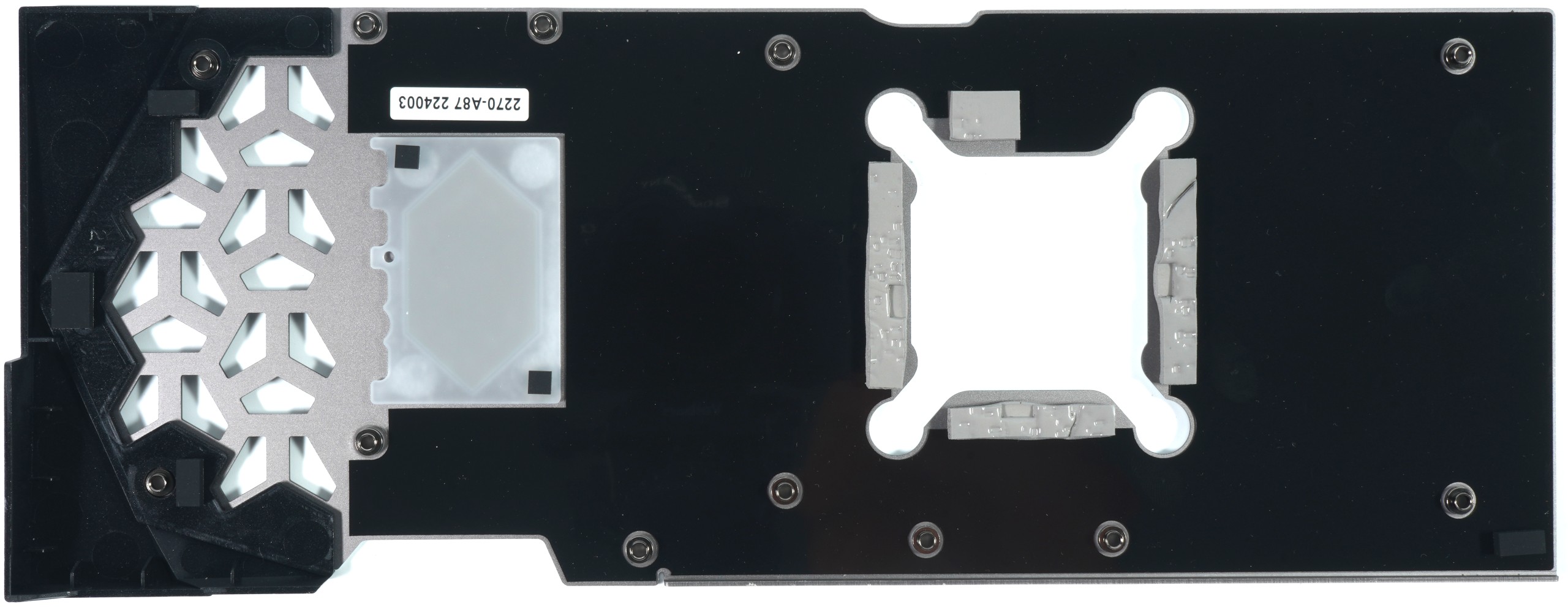
The pads used are extra class, well malleable, but still somewhat brittle. Since they adhere very well, disassembling the card is not without its problems, as the pads are damaged for the most part and have to be completely replaced when reassembling. Very good, reasonably soft pads with a thickness of 1.5 to 1.75 mm should be used here. We already know the three 10 cm fans with 10 rotor blades each from the older SUPRIM-X models. It fits like this.
The backplate still passively cools a part of the GPU socket, but not more.

- 1 - Introduction, unboxing and technical data
- 2 - Test system in the igor'sLAB MIFCOM-PC
- 3 - Teardown: PCB, components and cooler
- 4 - Gaming performance
- 5 - Power consumption and load balancing
- 6 - Peaks, transients and PSU recommendation
- 7 - Temperatures, clock rate, fan speed and noise
- 8 - Efficiency, summary and conclusion


102 Antworten
Kommentar
Lade neue Kommentare
Urgestein
Veteran
Urgestein
Urgestein
Veteran
Mitglied
Urgestein
Mitglied
Urgestein
Mitglied
Veteran
Veteran
Neuling
Urgestein
Veteran
1
Mitglied
Urgestein
Veteran
Alle Kommentare lesen unter igor´sLAB Community →