


Teardown and PCB analysis
The M.2 heatsinks can all be removed individually, which is handy if you want to upgrade to an M.2 SSD, for example, and a GPU is already installed. The CMOS battery is also relatively easy to access under one of the heatsinks, making it easy to maintain, although a few centimeters lower would have been even better for access with dual-slot GPU coolers. All M.2 slots have pre-installed thermal pads on the removed heatsinks, but there is also an aluminum strip with a thermal pad under each of the SSD slots so that the back of the hot media is also cooled passively as well as possible.
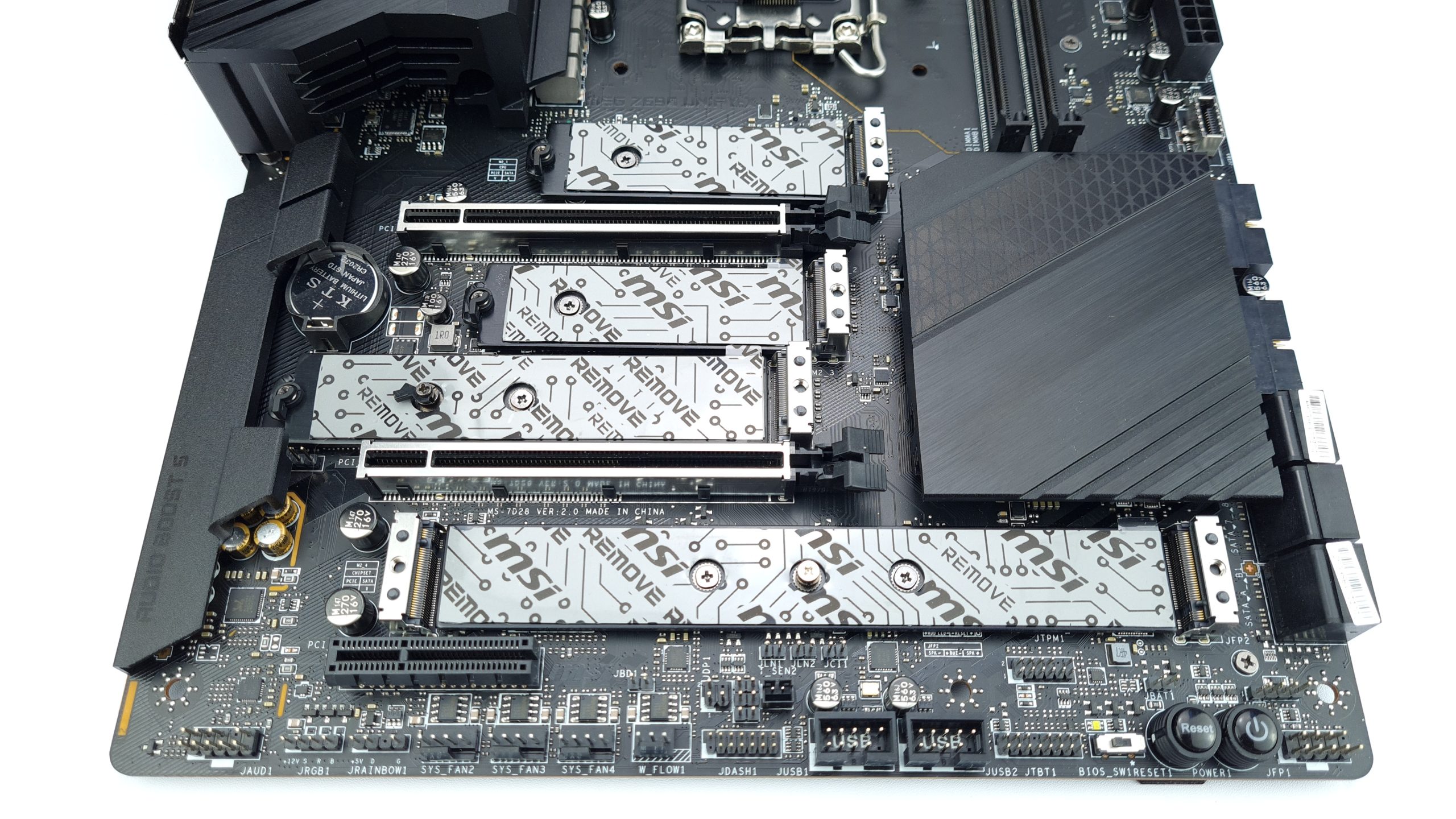
As with all Z690 boards, the upper slot is directly and dedicatedly connected to the CPU with x4. All other M.2 slots are connected via the chipset, so lanes are not stolen from the x16 slots for the graphics cards. All M.2 slots run with PCIe 4.0, except for the one on the bottom left, which can only handle PCIe 3.0. There is also a Thunderbolt 3.0 port between the internal USB 2.0 ports and the BIOS switch on the lower edge, in case you want to upgrade with a corresponding expansion card.
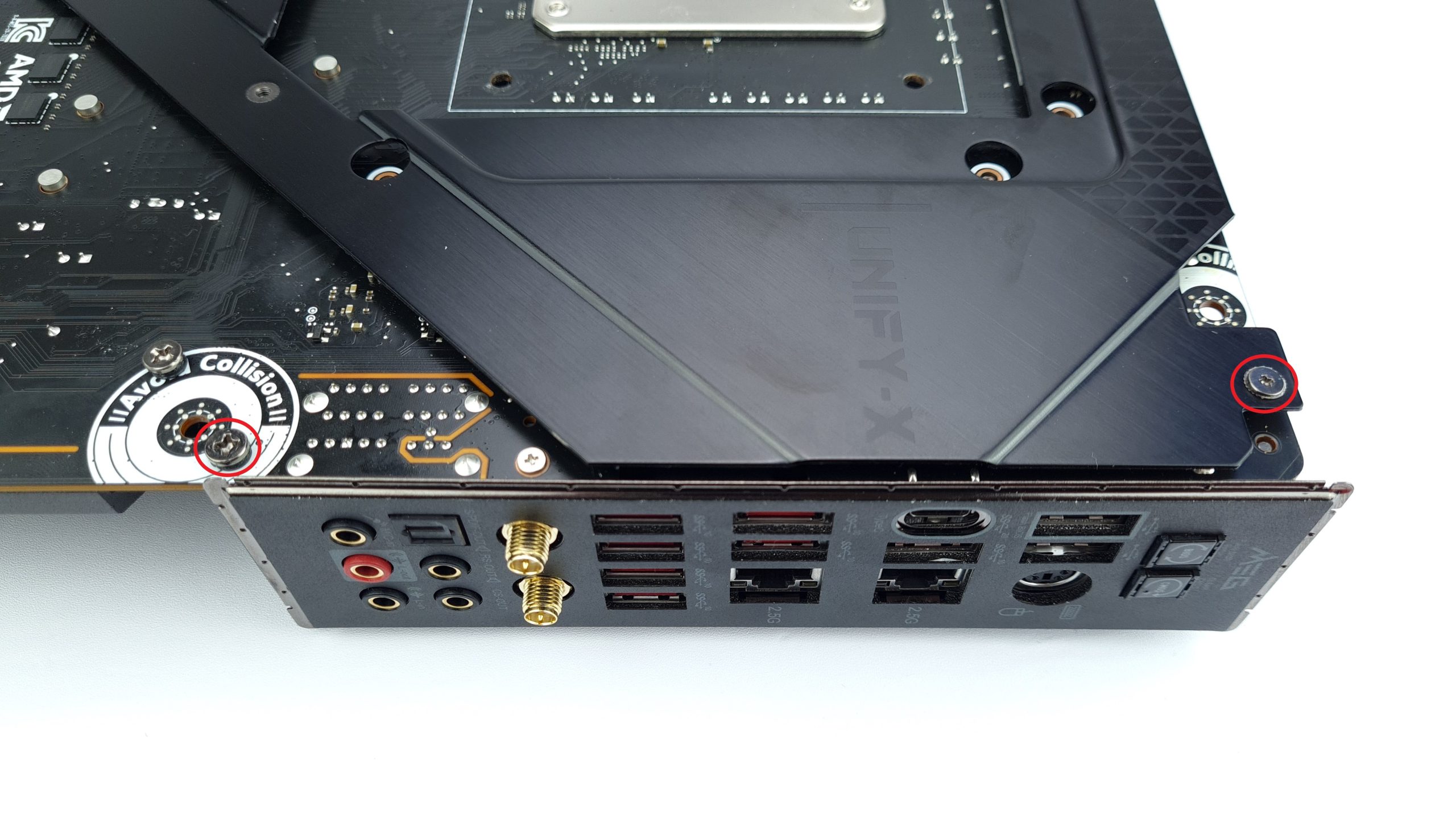
The heatsink of the voltage regulators is a large L-shaped component. For disassembly, in addition to the 4 large screws, two at the ends of the IO panel must be removed on the rear side, marked here in red. However, the backplate, other heatsinks and the IO panel do not have to be removed, which makes the VRM cooler very easy to remove.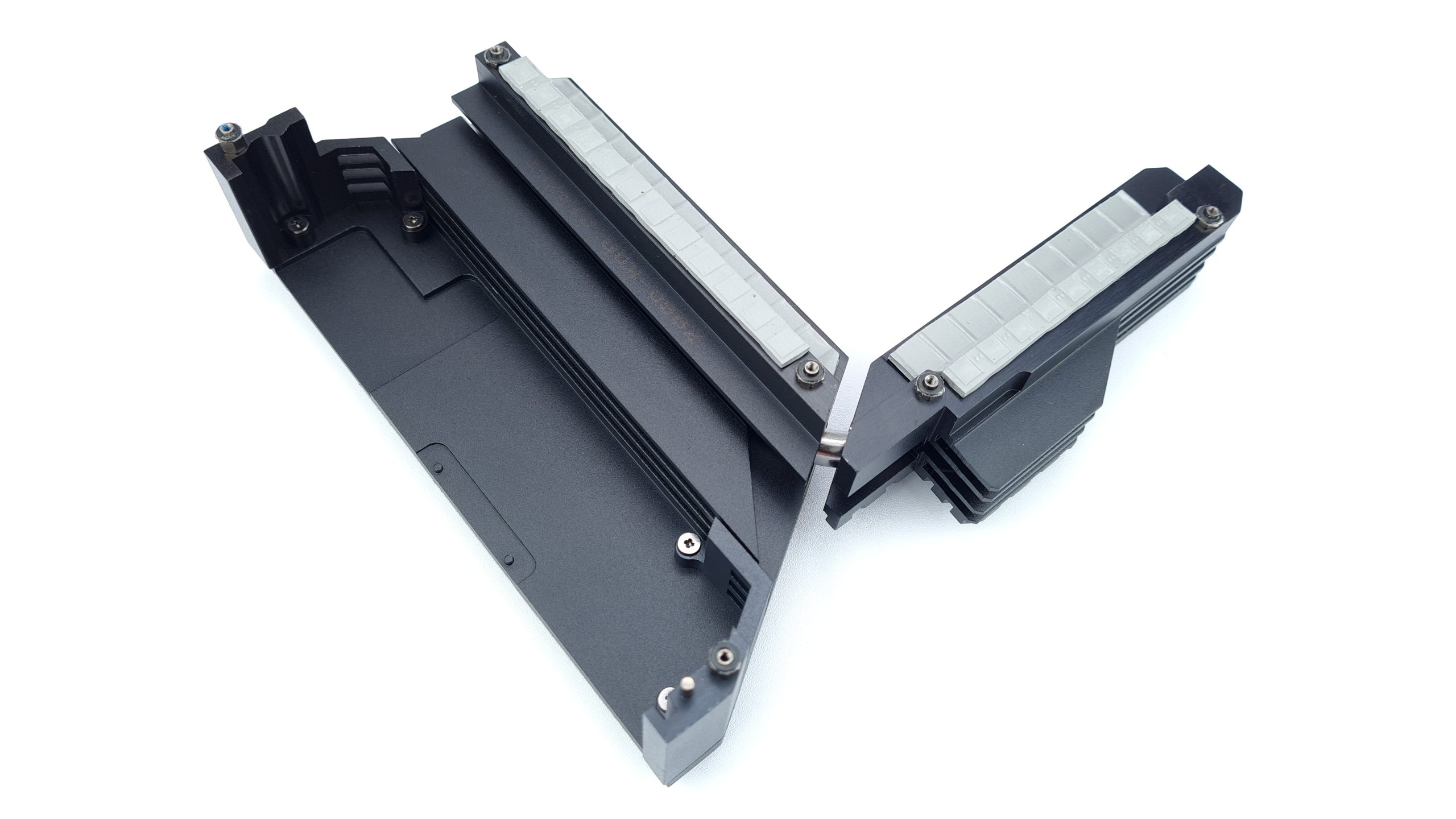
The heatsink consists of two milled aluminum blocks that are anodized black and connected by a heat pipe. Thermal pads, each 1 mm thick, ensure contact with the inductors and power stages and thus their cooling.
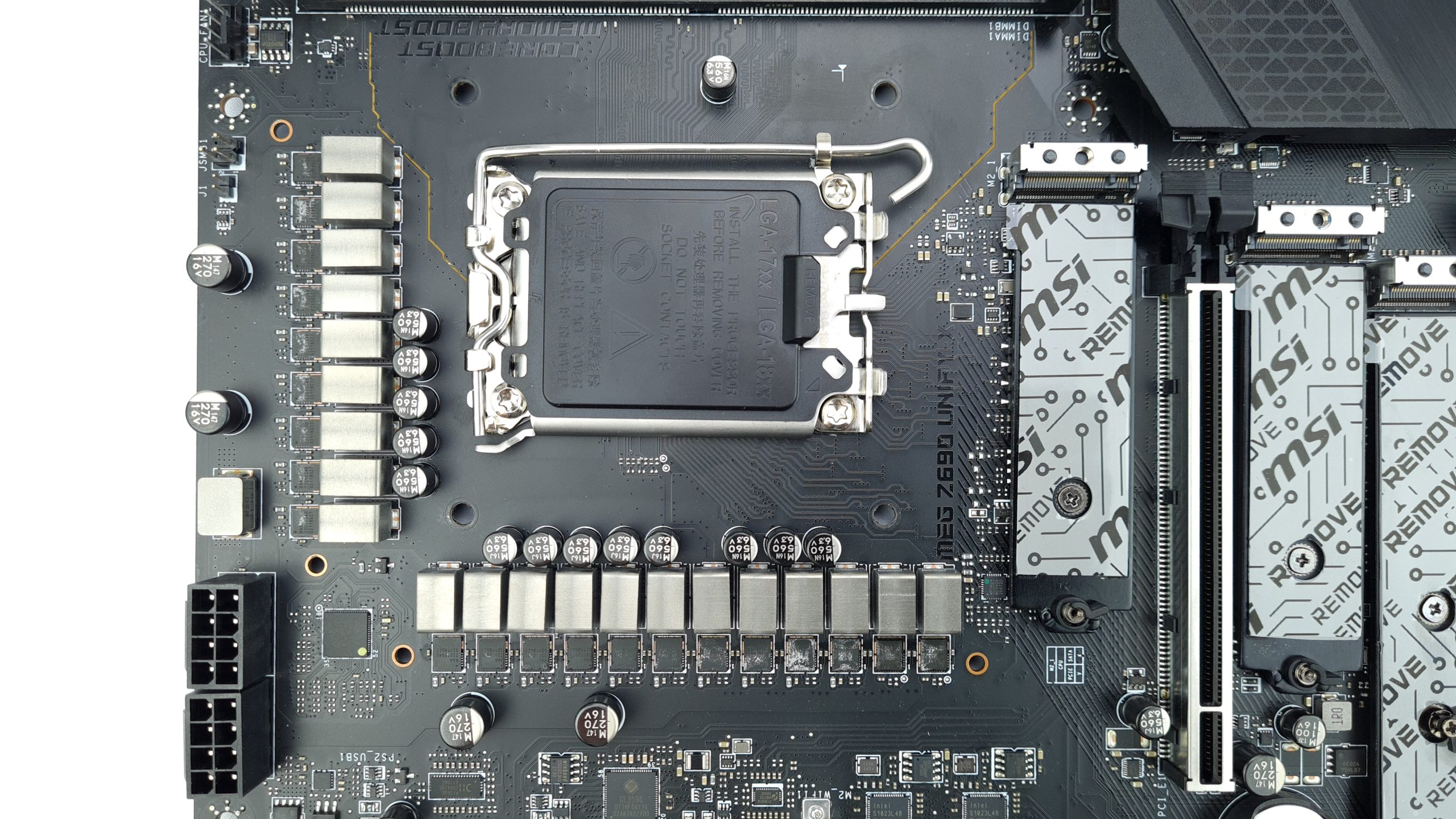
Speaking of which, MSI has given the board 21 of each, in a 19+2 phase configuration. Mind you, these are actually real, individual phases, not a duplicated marketing slogan. In contrast to the lush converters, MSI is a bit more frugal when it comes to filtering, both on the input and output side. 4 x 270 uF 16 V and 13 x 560 uF 6.3 V aluminum polymer capacitors are distributed around the socket on the front of the board.
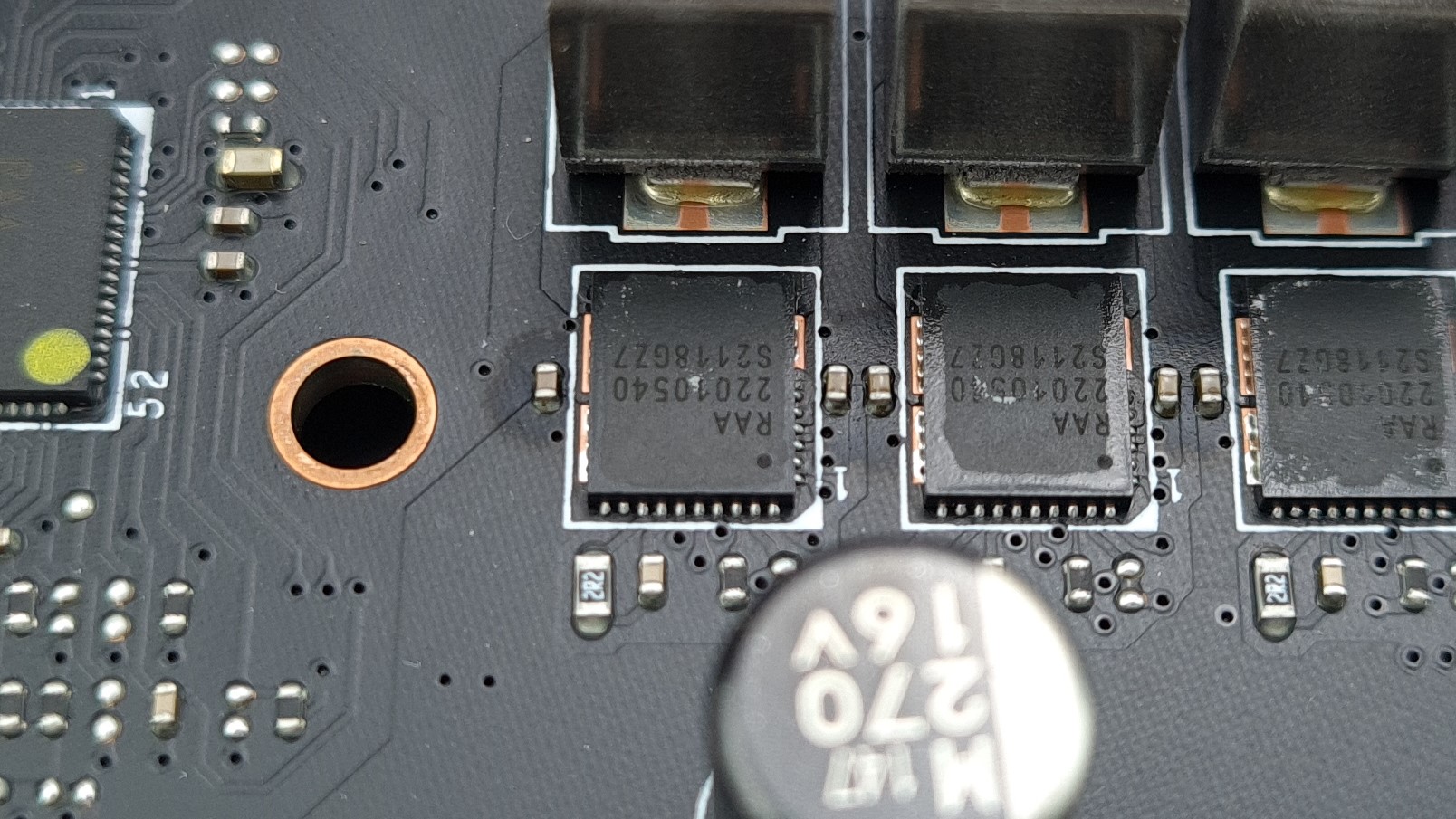
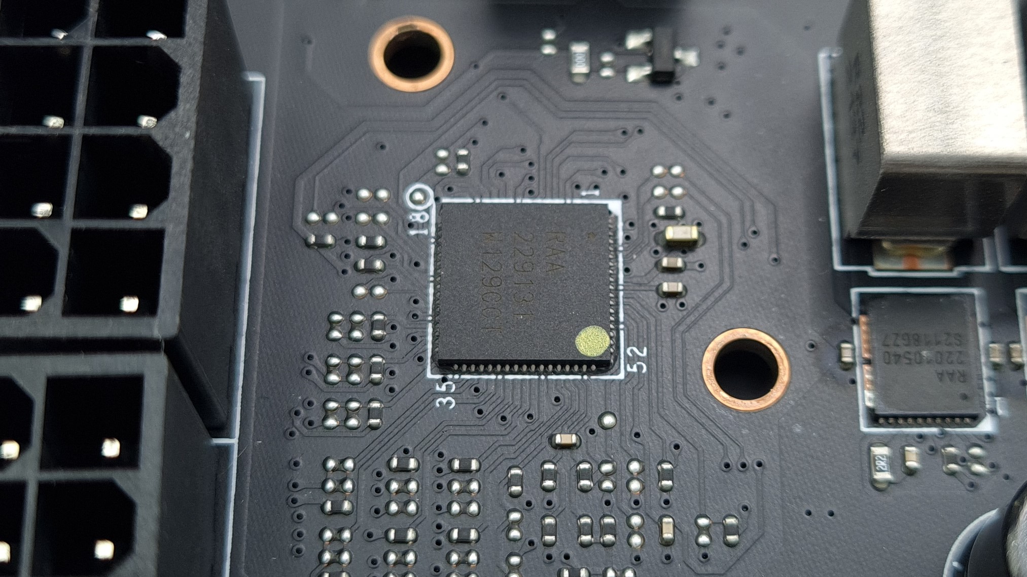
The voltage converters are Renesas RAA22010540 Smart Power Stages with a rated current of 105 A. Even if these components aren’t intended for such high currents in reality, you can already roughly estimate in your head that 19 of these components won’t have any problems with a heavily overclocked i9 CPU.the phases for Vcore are controlled by a Renesas RAA229131 PWM controller, which would even be capable of 20 phases.
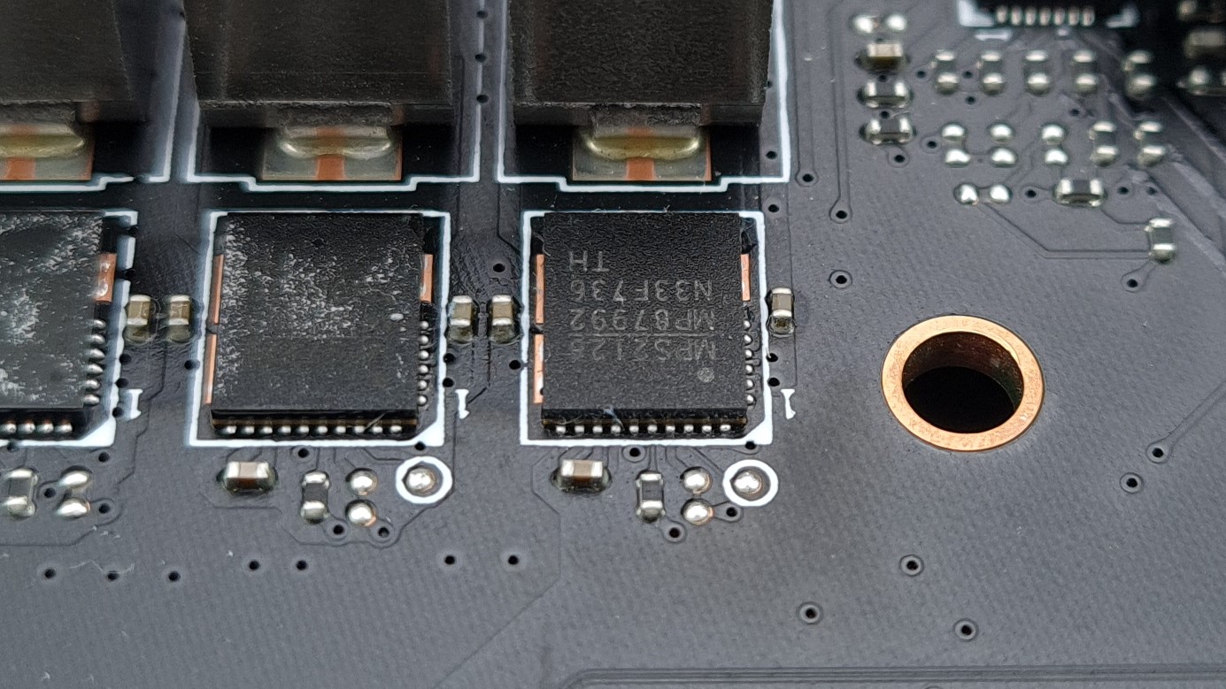

The remaining +2 powerstages are responsible for the VCCIN voltage (FIVR), using MP87992 70 A PLCs, controlled by an MP2940 2-phase controller, both from Monolithic Power Systems. Here If you want to know more details about the power supply and efficiency calculations, I recommend buildzoid’s PCB breakdown for the Z690 Unify-X.
MSI has also made a more frugal decision with the capacitors inside the socket and on the back, so that only MLCCs (multilayer ceramic capacitors) are used here and not SP caps (aluminum electrolytic capacitors) as is often the case. But this need not be a bad sign, because if the voltage converters already provide a very clean voltage supply by themselves, smoothing afterwards is of course only necessary to a small extent.
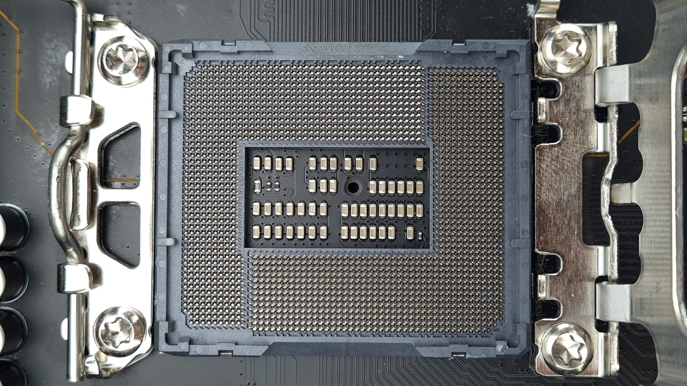
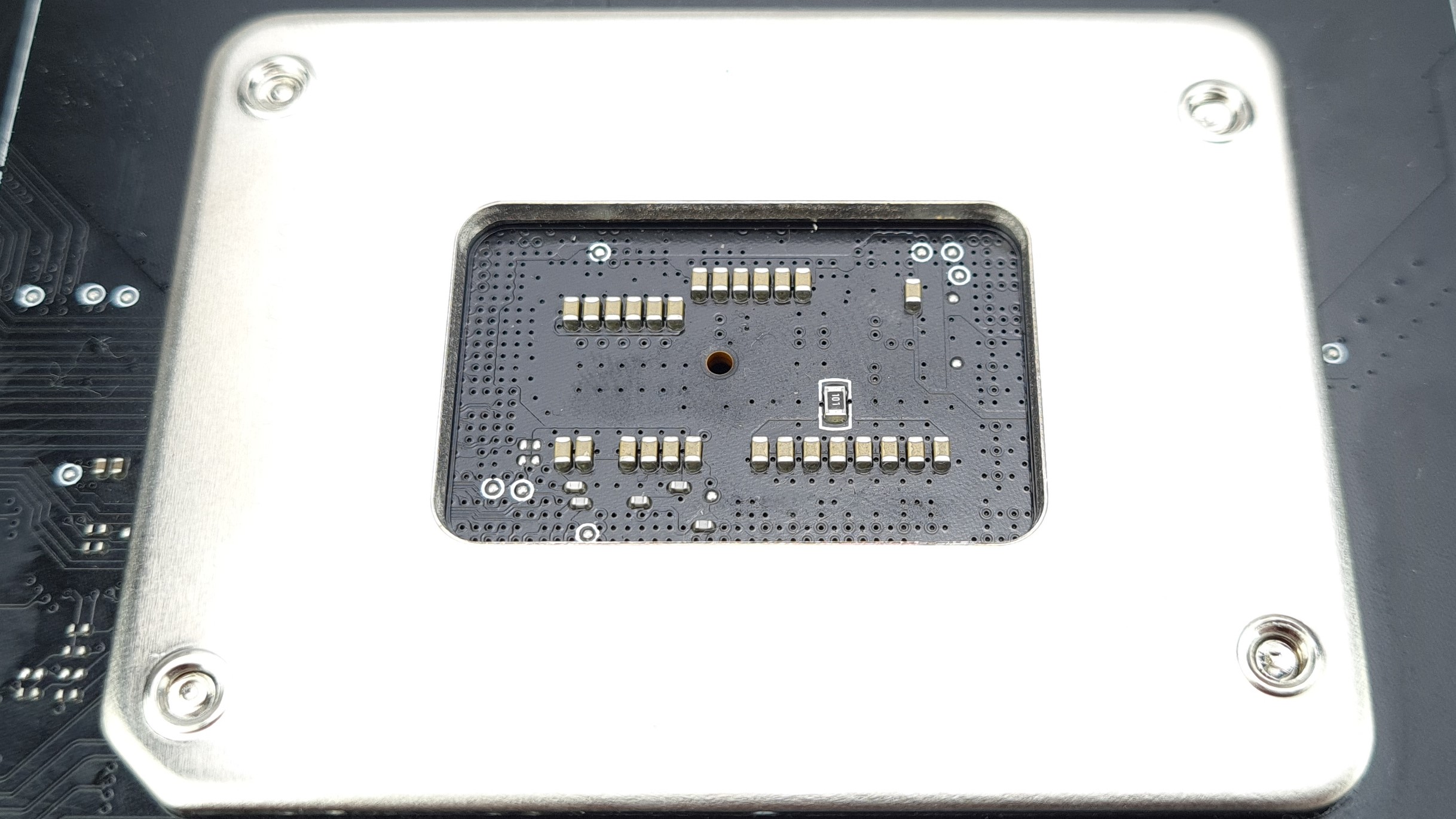
There is also a small hole in the center of the base to attach a temperature sensor to the bottom of the CPU from the back of the motherboard, especially relevant for XOC at freezing temperatures. The LGA1700 socket and ILM are made by Foxconn. Experience has shown that the “Washermod” can cause problems from 0.8 mm onwards with this type. In my sample, however, the screws were long enough to be able to integrate even the ideal 1.0 mm. This is how all further tests were then carried out.


5 Antworten
Kommentar
Lade neue Kommentare
Urgestein
Veteran
Veteran
Veteran
Veteran
Alle Kommentare lesen unter igor´sLAB Community →