


Teardown
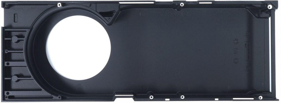
The case, or rather the solid case cover as a support, was made using die-cast aluminum and is relatively easy to remove if you have the two matching Torx screwdrivers. The slot bracket should also be removed to make it easier to remove the board later. But there is no need to write much about the value of the solution, which is quickly justified visually and haptically.
Underneath is the circuit board, on which both the cooler and the fan module are fixed with four screws and a clamping cross. The fan module, whose carrier plate is also made of light metal, covers the soldering areas for the two 8-pin sockets, so that one relies here on a separate socket at the end of the card, which was easily fixed with adhesive tape on the fan module.
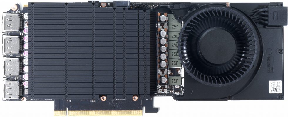
The fan module with the 6.5 cm fan is quickly removed and then reveals the board, which has no higher components in this area. This is kind of like a Sokoban for adults and we also see that the longitudinal chokes of the two interconnected inputs are also very shallow. The right row of voltage converters is thus cooled directly by the fan module, while the rest sits under the actual cooler. This is quite an interesting, but very effective solution.
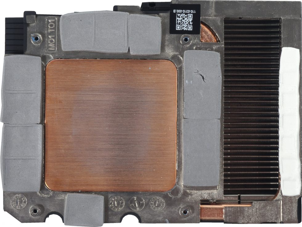
The cooler relies on a large, heavily ground copper heatsink as well as surrounding heat pipe elements for transporting the waste heat from the left voltage converter row to the cooling block (here mirror-inverted and therefore visible on the right under the bright heat conduction pad) and the total of 12 memory modules. Compact, but effective, because here, after all, around 200 watts are dissipated. The approx. 10 to 15 watts of board losses and the voltage transformers under the fan then count extra.
Circuit board and power supply
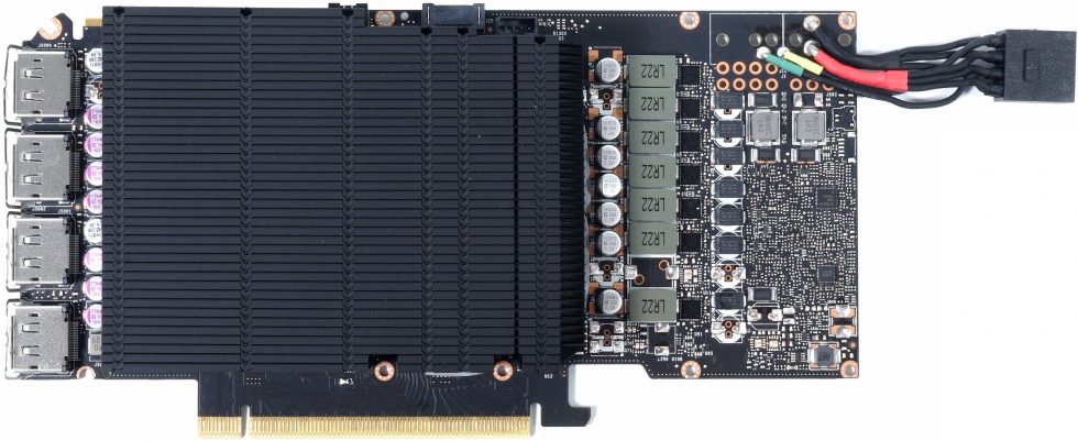
The circuit board is quite interesting and doesn’t really match any of the consumer boards exactly. It still most closely resembles the reference board of the GeForce RTX 3080, but there are definitely differences in detail and in the voltage supply distribution. One has accommodated a lot here on 21.2 cm length and the superposition also shows that, for example, a water block that fits on a reference board of the GeForce RTX 3080 could also fit here if the leave-out areas were implemented cleanly.
The board is based on the aforementioned PG132 reference design, a 12-layer backdrill board, but has been modified. The division of the main voltage supply into two parts was maintained. NVVDD stands for traditional core voltage, which is what we like to call GPU voltage. Here, there are a total of eight individual phases (one less than on the FE) provided by a uP9512R from UPI Semiconductor on the rear panel. This is a digital PWM controller with VID interface, compatible with NVIDIA’s Open VReg specification. These phases are each fitted with slightly cheaper 50-A powerstages AOZ5239QI from Alpha & Omega, which do not allow true MOSFET DCR, but do provide temperature protection circuitry and a readout output.
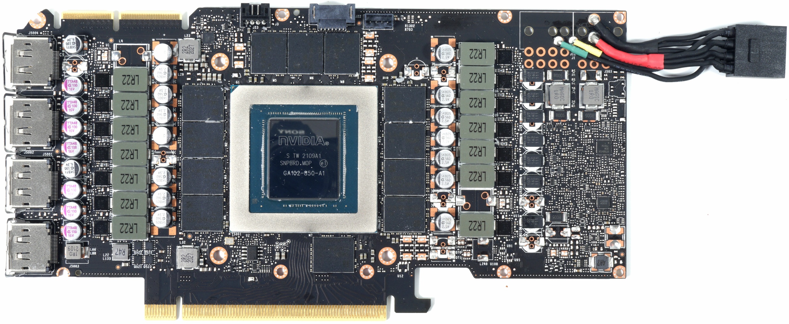
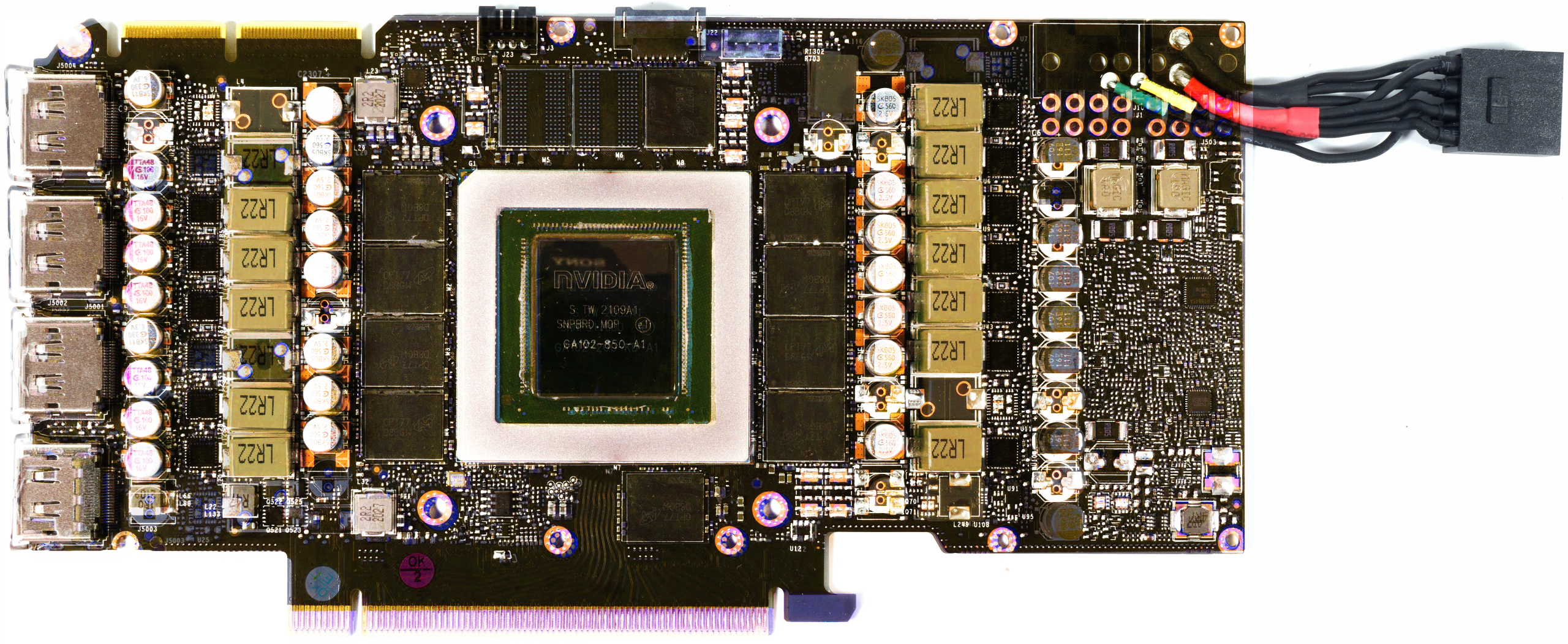
The assembly of the second GPU power supply MSVDD, which I had called “Gedönsspannung” and which stands for “Miscellaneous”, is very similar. We find a total of four individually controlled phases generated by an RT8845A. The powerstages are AOZ5311NQI, slightly stronger 55A models from A&O. So in the end there are 11 phases just for the GPU and the different voltages to the same. This should also make power gating in the GPU a bit easier, with AMD using a similar, albeit much smaller, offload with VDDCI. The voltage range of both ranges is between 0.7 and a maximum of 1.2 volts, whereby the maximum value can never be reached by the end user without special firmware and software. However, the minimum value is important, so there are technical limits for undervolting, but NVIDIA assigns them for all.
For the memory, NVIDIA uses two stages, which also rely on the familiar power stages of Alpha & Omega. However, the PWM controller (RT8845A) is located on the front The power stages of the PCI Express voltage PEXVDD and the 1.8 Volt are located on the front along with the corresponding coils. The capacitor six-pack on the bottom of the BGA contains two MLCC combinations and four SP-CAPs, will do. For input smoothing three coils with 1 µF each are used, behind which a shunt is connected. The voltage drop of the shunt is measured by a uS5650 from UPI.

- 1 - Introduction and technical Data
- 2 - Test System and Methods
- 3 - Teardown: PCB and Cooler
- 4 - AutoCAD 2021
- 5 - Solidworks 2021 (No FSAA)
- 6 - Solidworks 2021 (FSAA Enabled)
- 7 - Inventor Pro 2021
- 8 - 3ds Max, Catia,Creo, Energy
- 9 - Maya, Medical, Siemens NC, SW 2017
- 10 - DirectX 11, DirectX 12, Vulkan, OpenGL und DXR
- 11 - AI und Compute
- 12 - Rendering
- 13 - Power Consumption, Limits and Standards
- 14 - Transients and PSU Recommendation
- 15 - Clock Rate, Temperatures, Fan Speed and Noise
- 16 - Conclusion and final Words


29 Antworten
Kommentar
Lade neue Kommentare
Veteran
Urgestein
1
1
Urgestein
Urgestein
1
Veteran
Veteran
Urgestein
1
1
Urgestein
Veteran
Veteran
Veteran
Urgestein
Mitglied
1
Alle Kommentare lesen unter igor´sLAB Community →