


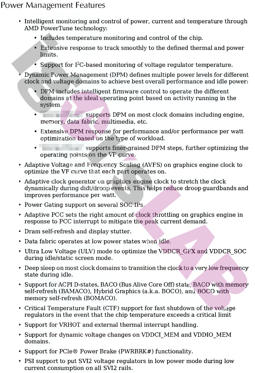
Power Management
According to the information available, PowerTune, DPM, AVFS and other well-known technologies are once again being used. I don’t need to verbally elaborate on that now, because the following insight into the slide is self-explanatory:
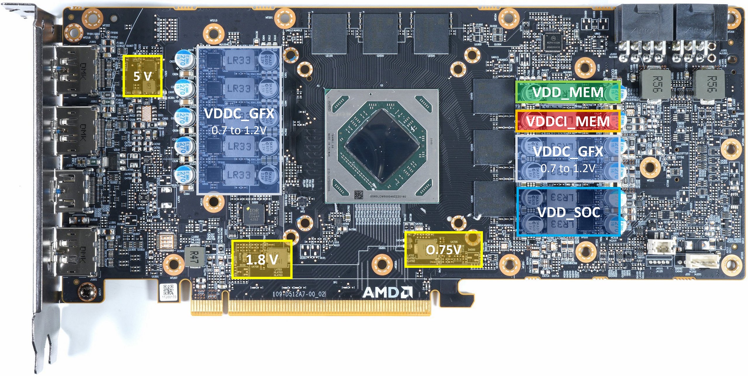
Power supply
For all those who always wonder where I get the details about the board analysis in my articles, I can again refer to the known basics for the Radeon RX 6600 XT, without having to quote directly from the slide, because nothing has changed. But it is quite interesting to mention these details as well. The supply voltages VDDCR_GFX and VDDCR_SOC shown by me in the schematics are assigned to one of the two SVI2 controllers in total, which is controlled by the SVI2 interface #0 of the chip. Here VDDCR_GFX is on the main domain of the controller and VDDCR SOC is on its second domain.
The supply voltage of the memory, i.e. VDDIO_MEM (which can be combined with VDDNDDQ of the memory devices on the board) and VDDCI_MEM are assigned to the other SVI2 controller, which is controlled by the SVI2 interface #1 of the chip. VDDIO_MEM (and VDD and VDDQ of the memory devices) are located on the main domain of the controller and VDDCI_MEM on its second domain. How this looked like with the Radeon RX 6700, I’ll show you with a known scheme from my launch article, because except for the number of voltage converters it should all be very similar:
It is also interesting what AMD writes about the TDC, because as a requirement for the voltage converters they state that the values set as maximum must be able to be held for at least 1 ms. This is important for a stable supply and also corresponds to what had already been assumed for the other cards. Better, longer, of course, is never forbidden.
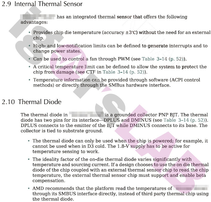
Temperature monitoring
It’s certainly interesting to know that they’re probably going back to the good old “GPU diode” as a feedback and indicator of chip temperature, rather than just extrapolated hotspots. The following two paragraphs also contain interesting tolerance ranges, which the general public certainly did not know in this form. Other details include the fact that the diode is powered by the 1.8 V source (see schematic above), which I always show on my board analyses and which is switched off on the Radeons in sleep mode.


21 Antworten
Kommentar
Lade neue Kommentare
Urgestein
Urgestein
Urgestein
1
Urgestein
Mitglied
1
Mitglied
Urgestein
Mitglied
1
Mitglied
Mitglied
Mitglied
Mitglied
Mitglied
Veteran
Alle Kommentare lesen unter igor´sLAB Community →