


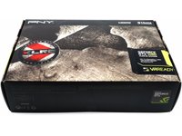
 With the GeForce GTX 1060 XLR8 OC Gaming, PNY offers a simpler model that focuses on the most moderate cost possible. Nevertheless, the factory clock has been raised properly and is otherwise quite optimistic about the performance of the card.
In direct comparison to the competitions, the card must now prove that this balancing act between a cheap offer and the wishes of the players really works satisfactorily. In any case, we are already curious, because the other cards of the XL8R series from PNY that have been tested so far did not leave a bad impression.
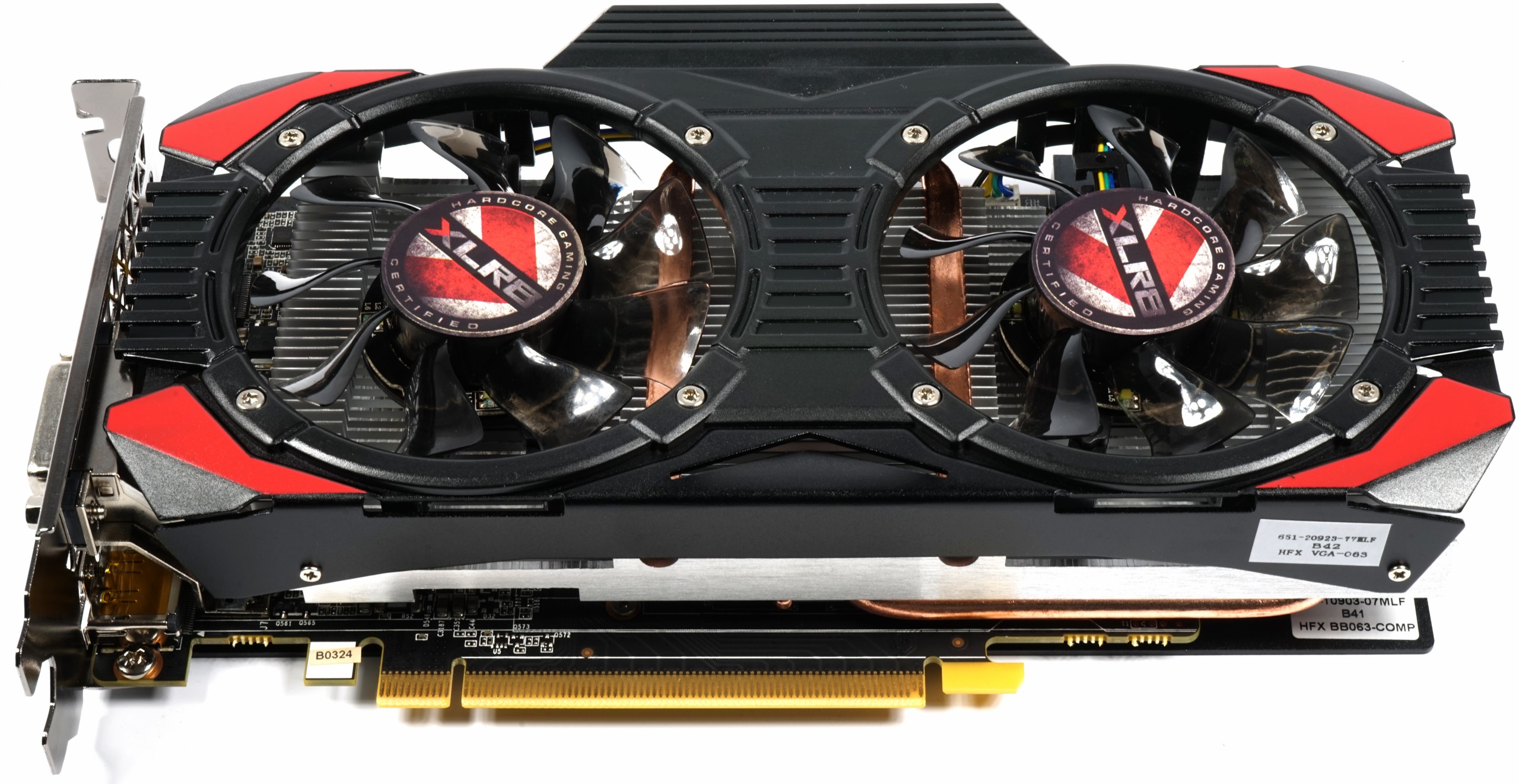
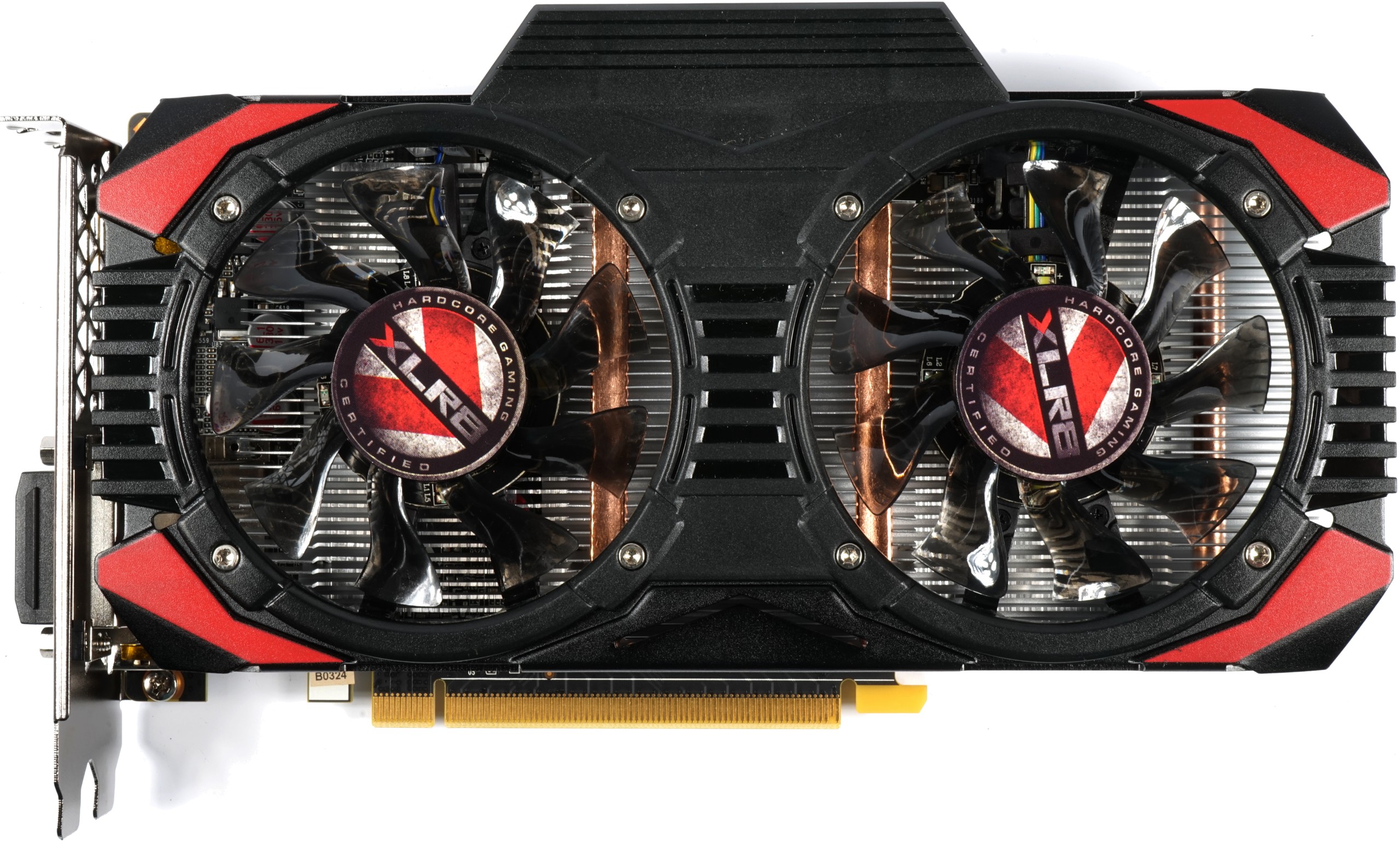
External structure and connections
The radiator cover on the top is made entirely of raven-black plastic, as well as various red-printed color applications and is neither exciting nor ugly, including the two 76 mm fan modules (opening 80 mm). Good optical average, which in addition to the fan openings, four optically outstanding screws were given each, which keep the whole thing on a skeleton of black powder-coated light metal. Can you leave and accept it.
The card weighs only 679 grams and is quite compact. It measures only 22 cm in length, is 11.7 cm high, 3.5 cm deep (installation dimensions) and thus occupies two slots.
 |
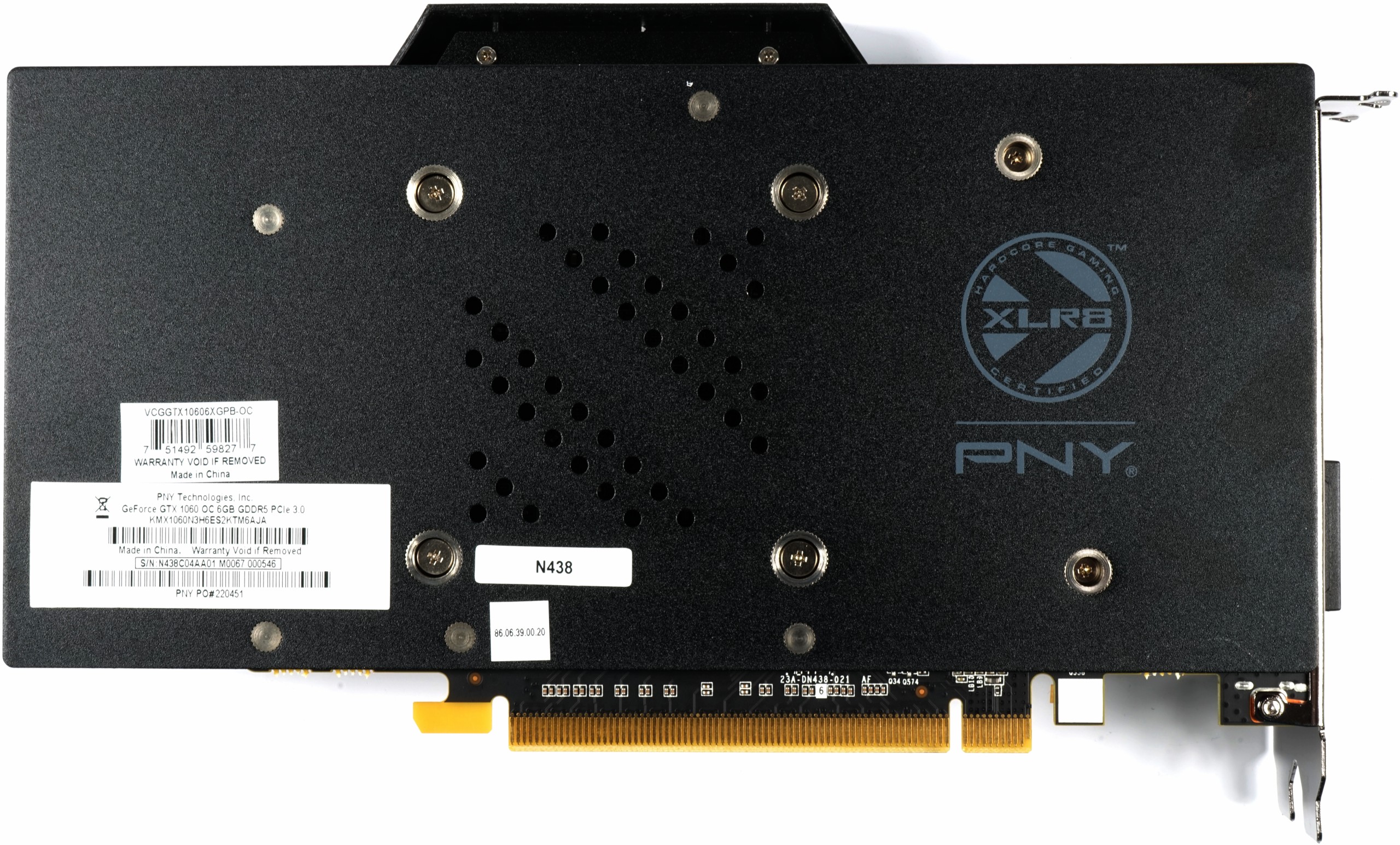 |
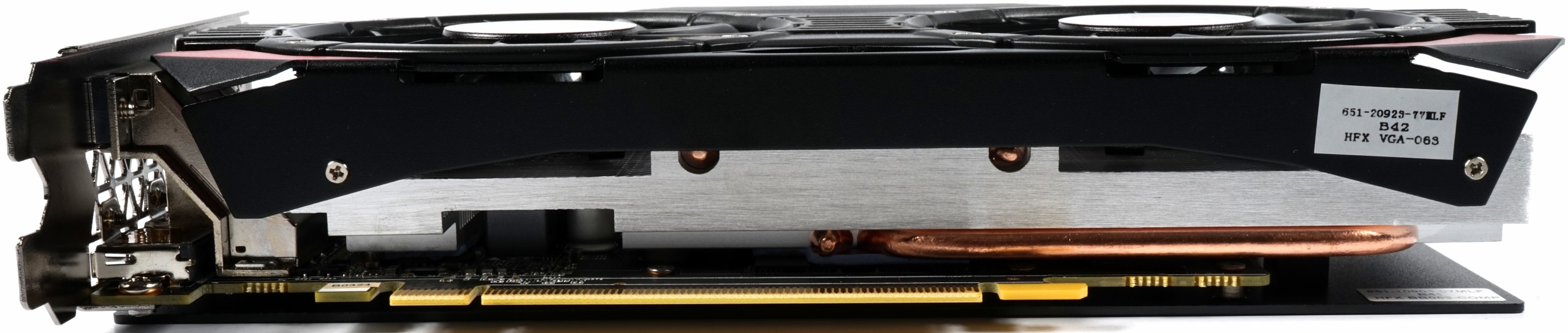
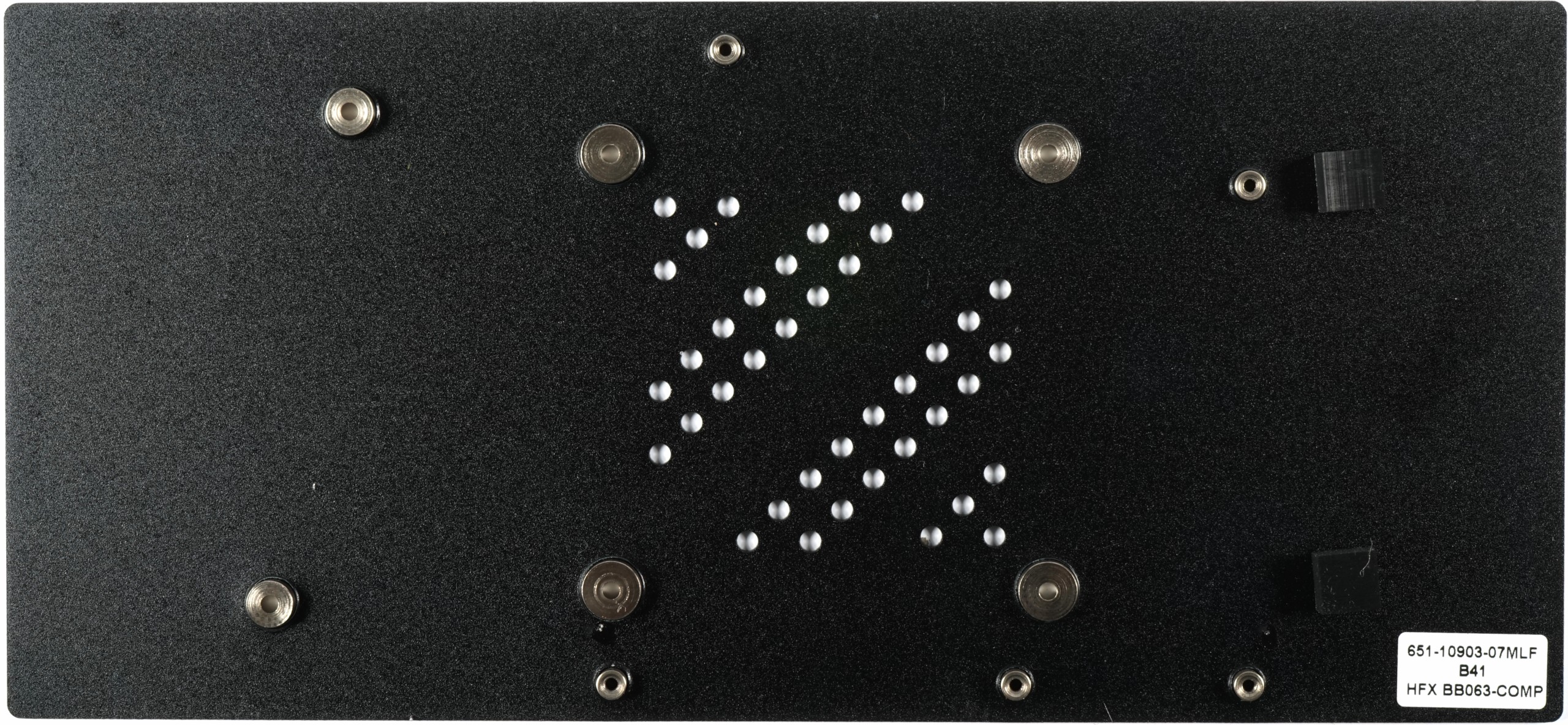
The back of the board is covered by a one-piece backplate, which has only a few ventilation openings and no cooling function. With this backplate, you have to plan another five millimeters depth on the back and take care, especially with ITX systems, that nothing conflicts between the CPU cooler and the card.
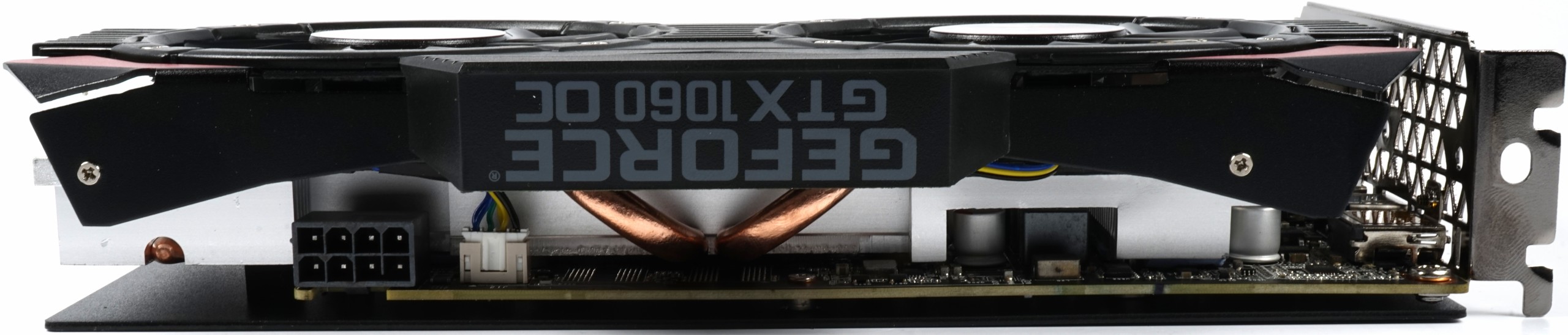
The top of the card has an imprinted Geforce GTX-1060-OC lettering. The 8-pin PCIe power supply connector sits 180° rotated at the end of the card. This makes technical sense, as you don't have to shorten the cooling fins any further.
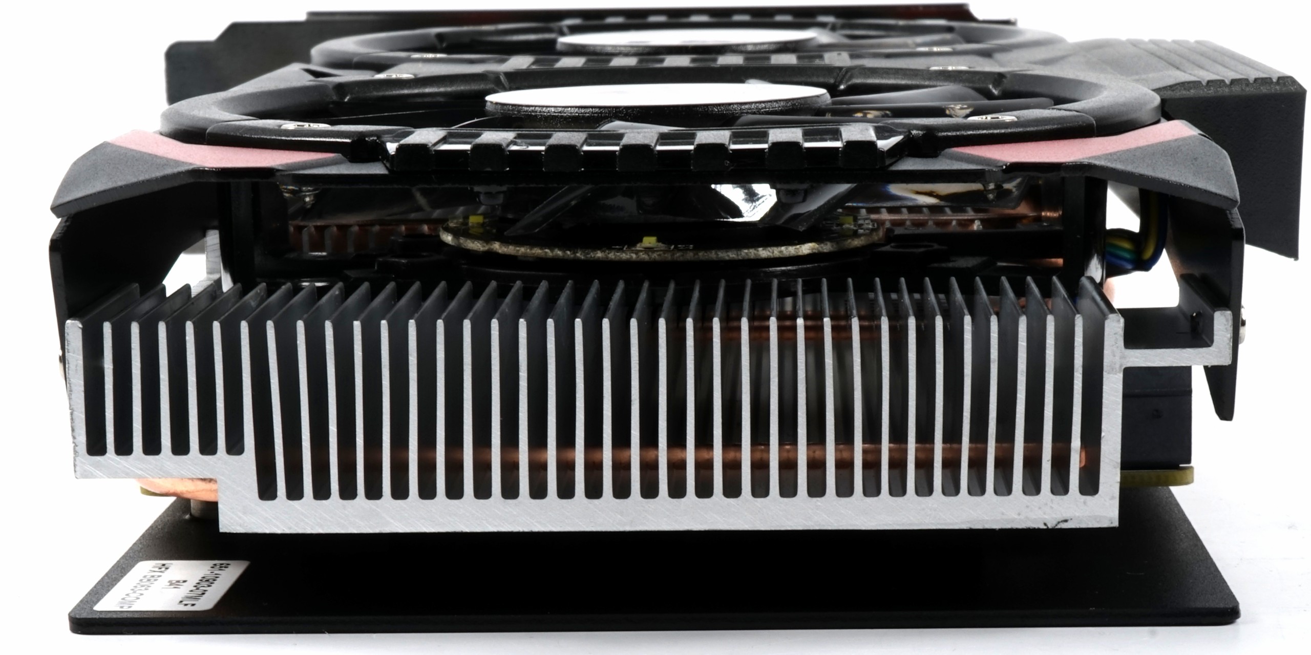
We can see very well from the sides that the heat sink is made of simple strandaluminium, from which the respective openings have been milled out. Two 4 mm heatpipes are designed to accelerate the removal of the resulting waste heat. We will come back to this in detail in a moment.
The horizontal slat alignment ensures that a not inconsiderable part of the waste heat is passed over the, thanks to the many honeycomb-shaped openings very air permeable, slot aperture is carried out of the housing. You can see this principle of air flow at the end of the map, but here the air lands in the middle of the housing, which makes a good airflow all the more important.
 |
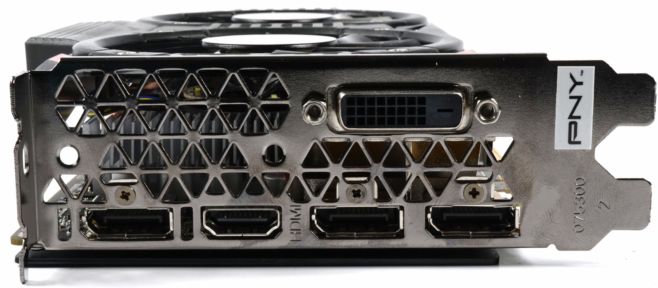 |
The slot aperture carries the usual five outputs, a maximum of four of which can be used together as part of a multi-monitor setup. In addition to the dual-link DVI-D (an analog signal is not looped through), there is an HDMI 2.0 output and three DisplayPort 1.4 ports on the back.
Board and assembly
Let's take a closer look at the PNY self-designed board, which has some distinctive features compared to Nvidia's reference and most other board partner cards.
First, we'll see the six phases, four of which are allocated to the GPU and two to memory. However, two of the GPU phases work as a capped load balancer that ensures that the motherboard port is not overloaded and standards are met, depending on the load. Which is probably probably three real phases in the end. So you can see that way, or so.
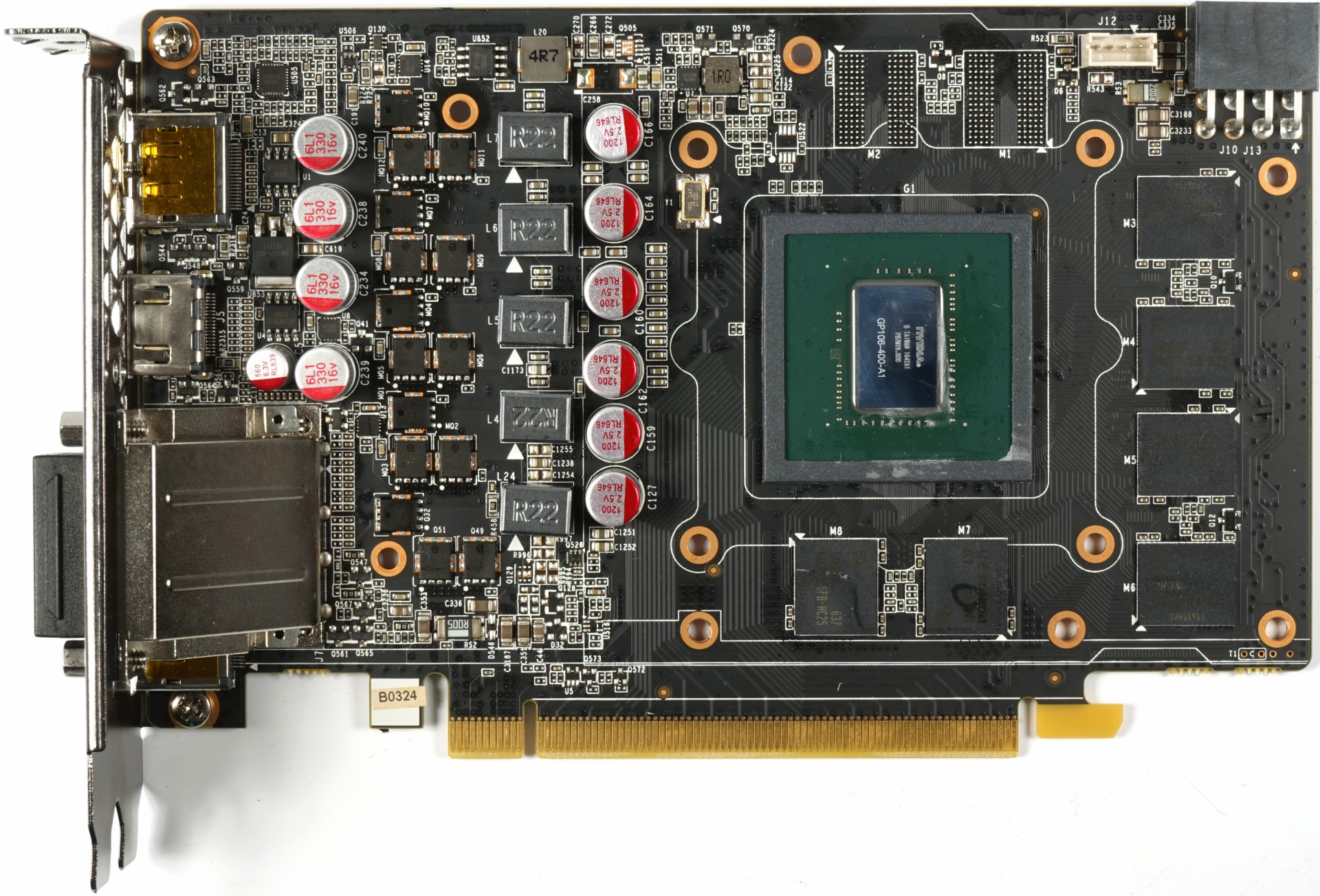
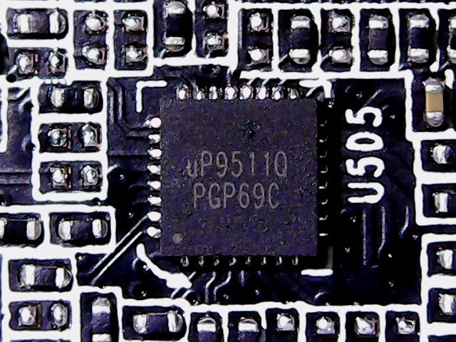
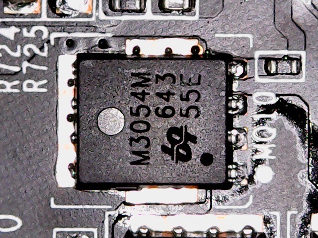
PNY uses a uP9511 from UPI Semiconductor as a PWM controller. All voltage control circuits, whether for the GPU or memory, are equipped on the high-side with an M3054 from UBIQ, a subsidiary of UPI.
 |
 |
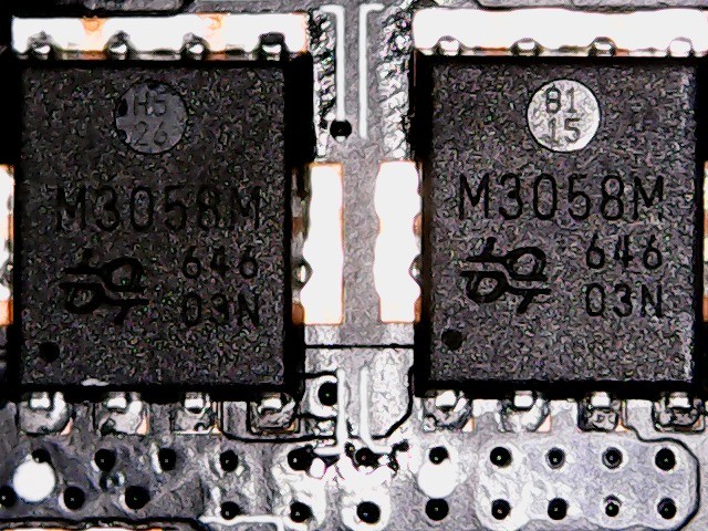
On the low-side there are two parallel operated M3058s from the same manufacturer. The encapsulated ferrite core coils are cheap average goods.
 |
 |
All in all, you can already tell that you haven't put the last penny into expensive components, especially since smoothing solids and coils are completely missing in the entrance area. This applies to all two 12V rails.
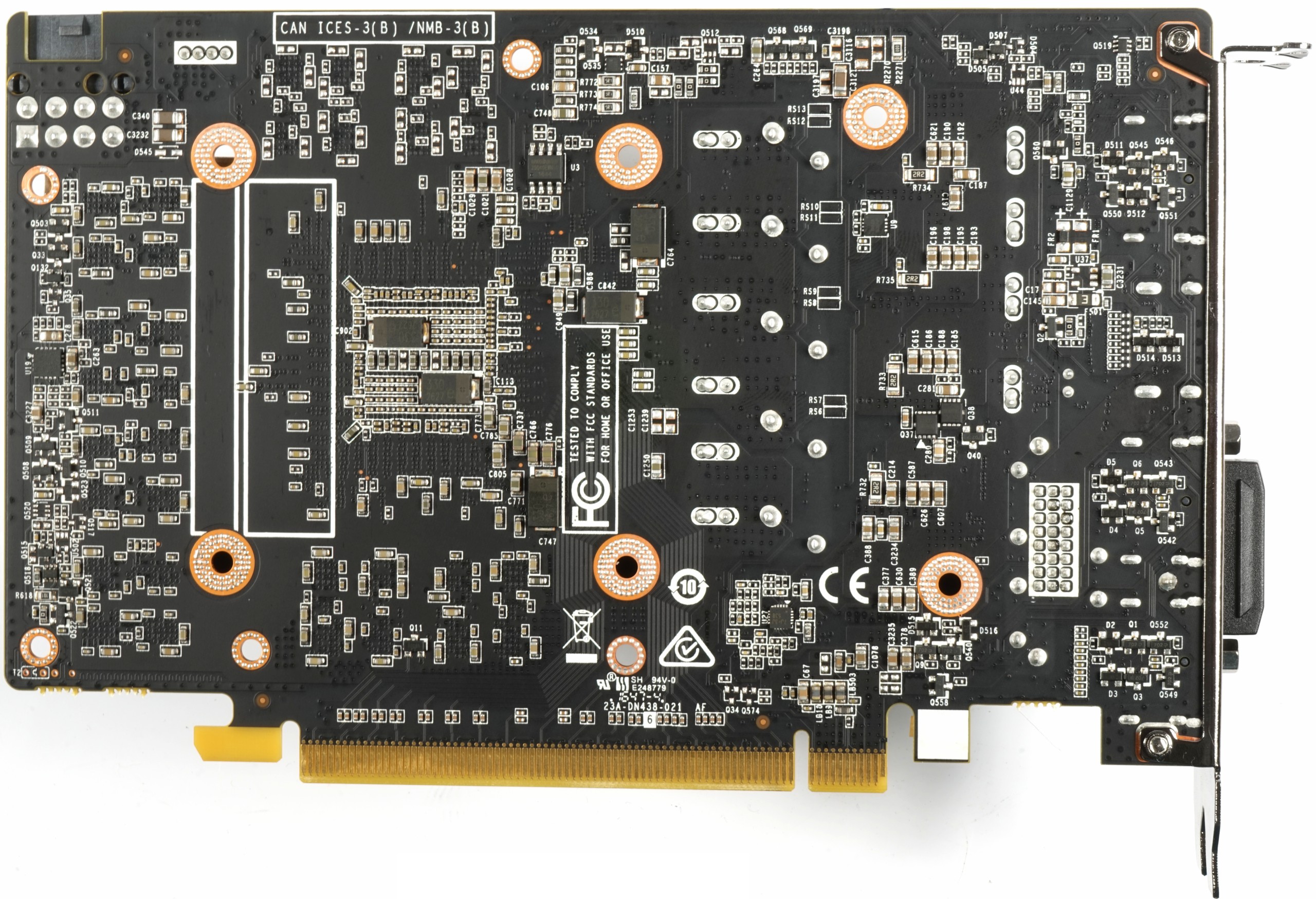
Below the GPU, two more capacitors are soldered to intercept and smooth voltage peaks – exactly the same principle as Nvidia's Refrenz.
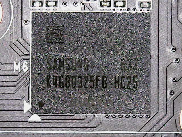
Again, we find that only six of the eight existing memory fields are filled with modules on this map. These are Samsung modules of the type K4G80325FB-HC25, each with a capacity of eight gigabit (32x 256 MBit) and can be operated with voltages between 1,305 and 1,597 volts, depending on the required clock. In total, this results in a total memory of six gigabytes.
Clock rates, voltages and power consumption
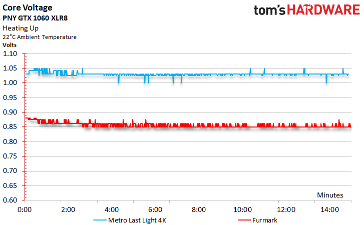
Of course, the course of boost clock and adjacent GPU core voltage as well as the connection between clock speed and voltage are also interesting, whereby the clock curve breaks down a little, but not dramatically, during gaming and when the card is fully warmed up.
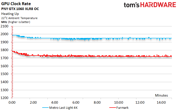
While the initial 2 GHz boost clock for the gaming loop falls to an acceptable 1949 MHz on average after heating and under load (smaller fluctuations up and down included), the measured voltage values look similar: average of 1,031 volts, although it can also fluctuate somewhat here.
This is due to the intervention of Boost 3.0 and the rather low-set Power Target, which limits the power consumption to 130 watts and below.
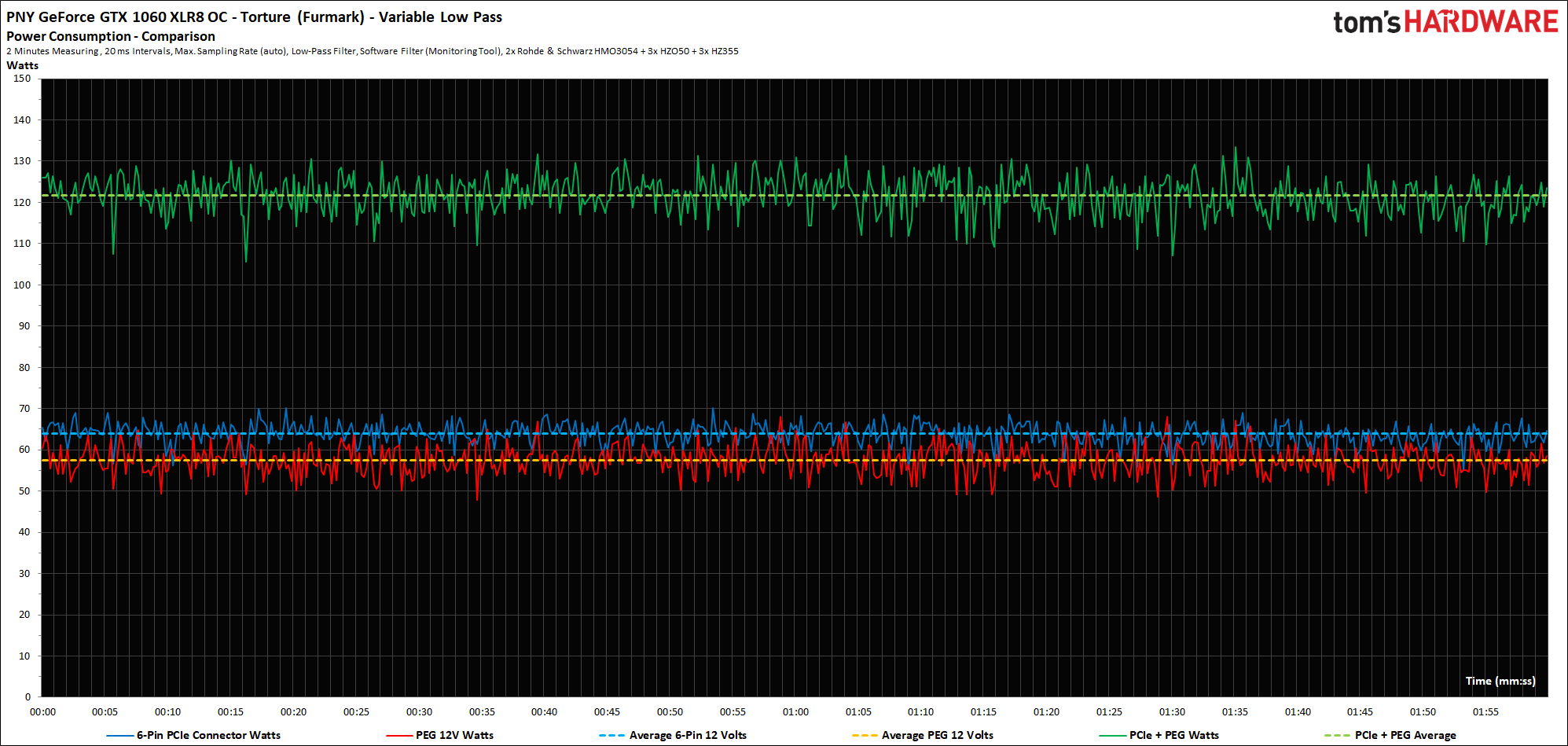
These voltage curves and the flowing currents result in the already mentioned power consumption, which we can measure very well with our exact equipment at all connections.
The lowest GPU clock speed for idle measurement is approx. 215 MHz. We worked with a variable low-pass filter for the measurements, so that we only mention possible, very short load peaks on the margins (greyed out bar), because they are hardly relevant in practice and have also irritated many readers.
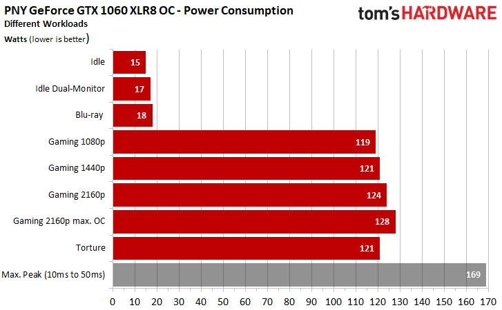
It is also the low Power Target that cuts the voltages during the stress test Boost 3.0 to such an extent that the power consumption is even slightly lower than in gaming, if you start the worst case there.
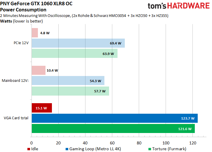
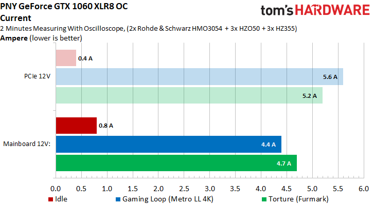
Loading of the power supply connections
Now we look at the division of the loads at maximum gaming load and the stress test: Since the 3.3V motherboard connection is not used at all, we have dispensed with this voltage rail in the diagrams.
The division of the phases between the respective supply connections is completely uncritical, but also leaves no greater room for overclocking tests according to the standards – but these are anyway provided by the BIOS (Power Target and Voltage Specification) braked:
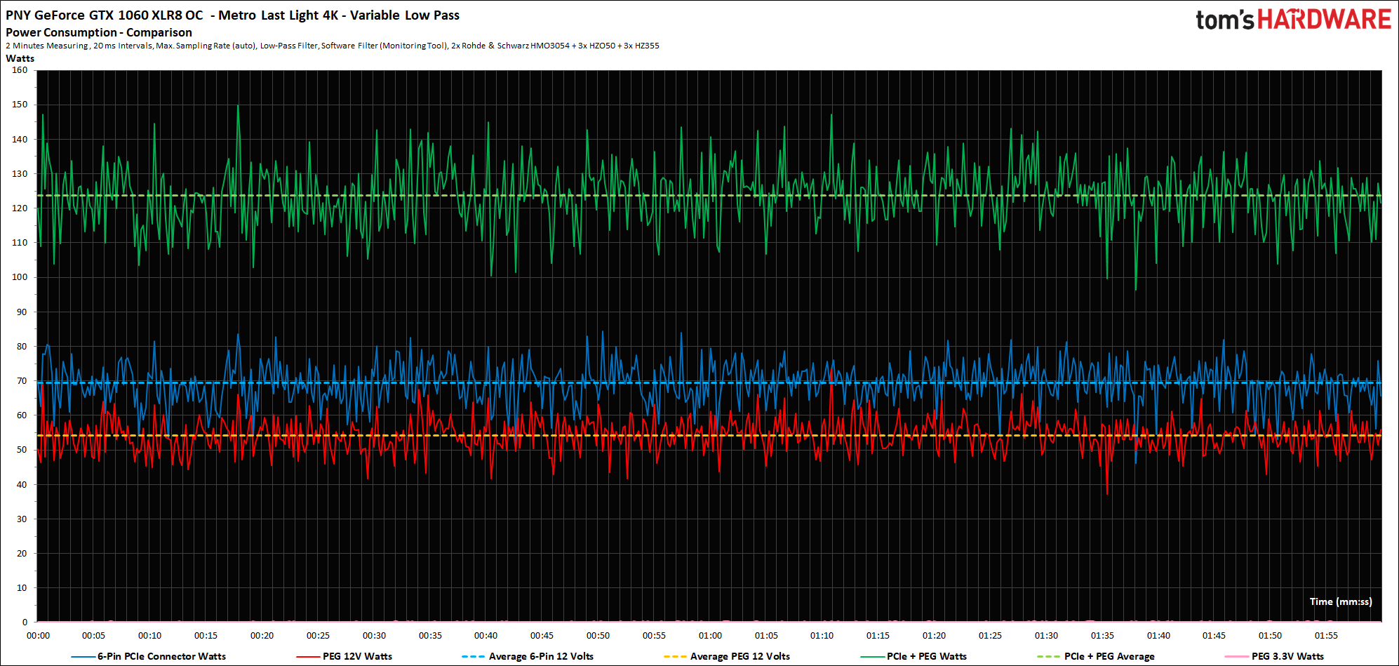
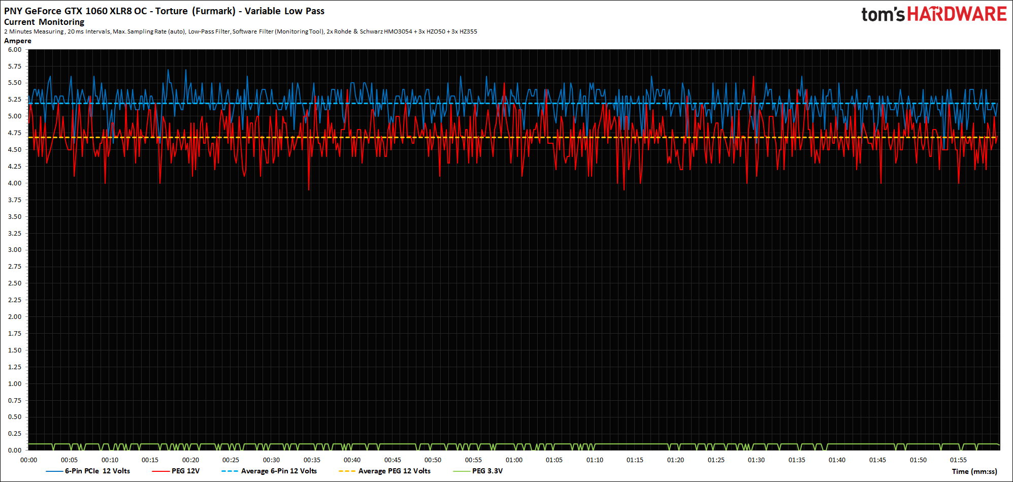
Here's another clickable diagram with the respective history curves for gaming and stress testing:
 |
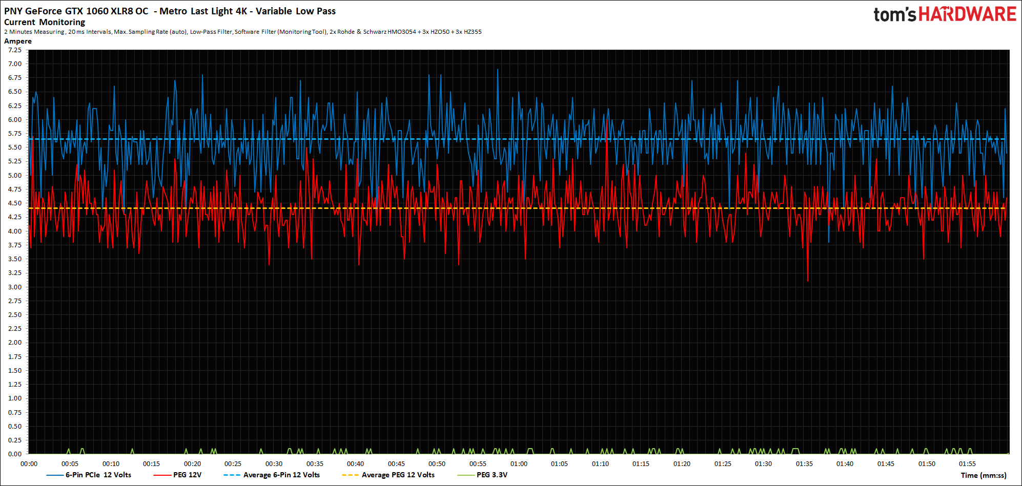 |
Since the standards (PCI SIG) refer only to the flowing currents, we now look at the following diagrams, because the power consumption is only half the rent. With around 4.7 amperes on the motherboard slot, however, you are always on the safe side (PCI-SIG standard: max. 5.5 ampere):
Of course, there are still clear large screens for the measured currents:
 |
 |
Cooling system and temperatures
Now we come to the cooler, which has hardly any special features. The backplate, which is not relevant for cooling, is purely optical in nature and is secured from the top of the board with a few screws against the overly curious.
The geometry of the total of nine 9 cm rotor blades, which are slightly wave-shaped at PNU, is designed for maximum airflow (and turbulence). The rotor blade surface is smooth and without grooves. As already mentioned, the rather chunky-looking cooler has horizontally aligned fins as well as two angled 4 mm heatpipes made of sintered composite material.
One of the beeps is circulating and dissipates the heat to both the radiator end and the top. The other, shorter heatpipe only leads upwards. Both heatpipes have been pressed and sanded in the aluminium cooler (DHT principle) so that they lie directly on the GPU.
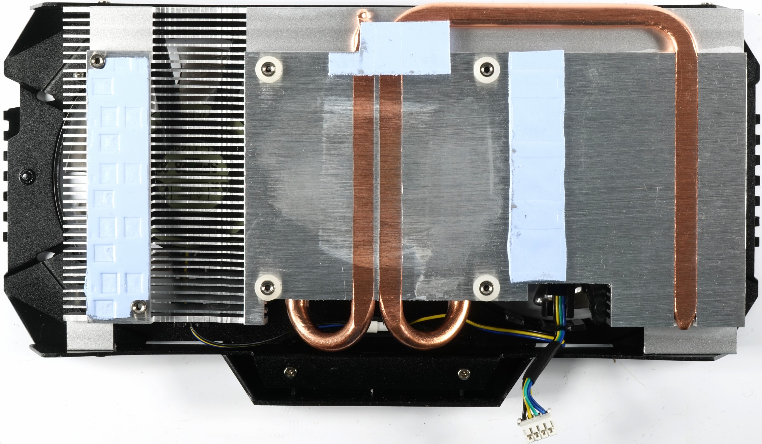
The area incorporated in the strand for the voltage transformer MOSFETs can be liked, but the coils have to do without active cooling.
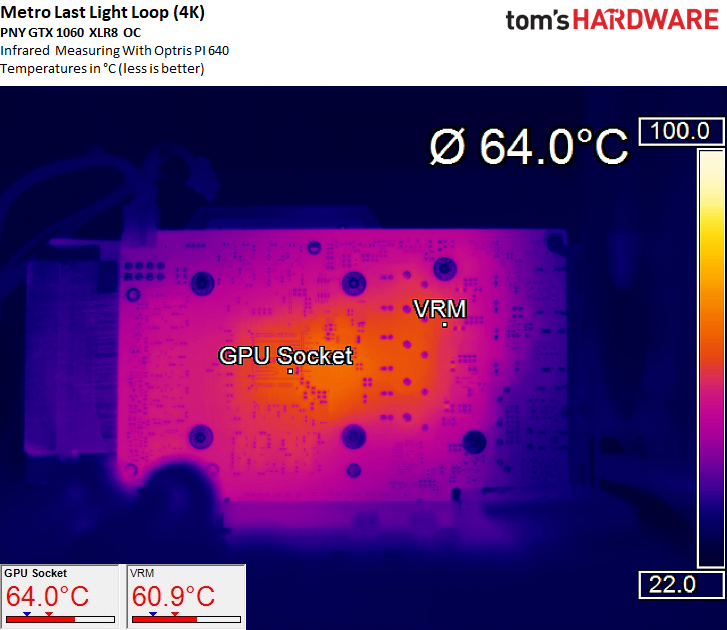
With the 64 to 65°C on the Gaming Loop (closed housing maximum 66°C) the cooler does its service perfectly, but at the end is correspondingly loud, as we will see in a while. So there is still plenty of room for manual fan rotation adjustments.
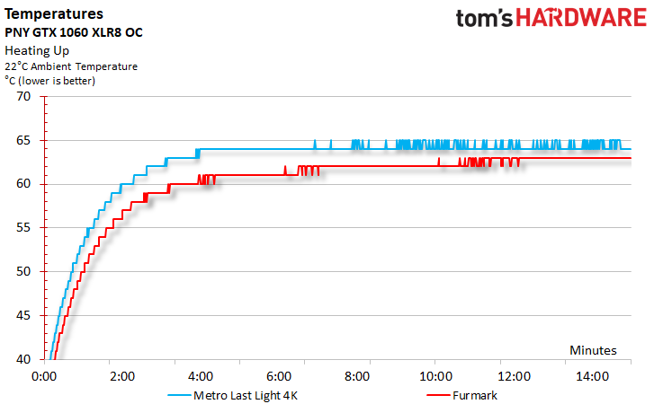
The measurements with the removed backplate show that the board stays really cool overall and even the hotspots are well below 70°C.
The stress test looks similar, especially since the power consumption is even lower than that of the gaming loop. This fits in any case and allows for huge reserves.

Once again, it turns out that simple solutions do not necessarily have to be the worst.
Noise
Hysteresis is not an issue for many manufacturers, PNY does not require a fan shutdown, permanent 50% fan speeds in idle mode as a minimum are anything but inaudible and we really wonder why 33% or less is not enough Had. Because in the idle, the card stays loosely below 30°C in this setting.
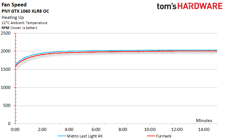
The noise in the idle is far too high at 34.7 dB(A) and unfortunately cannot be lowered further, because the fixed, far too high minimum speed in the firmware cannot be overwritten.
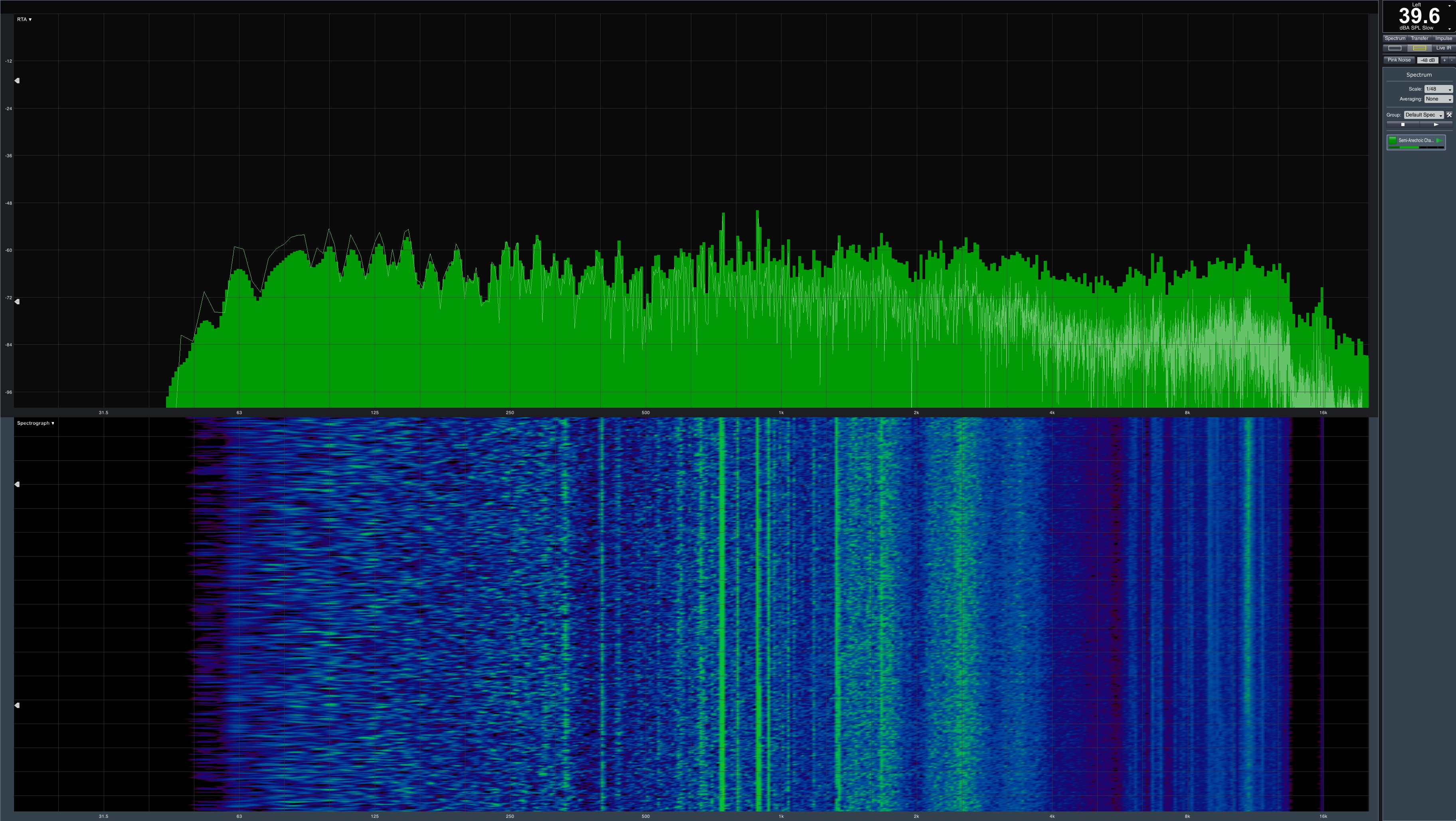 The noise of 39.6 db(A) under load is certainly still acceptable, but not a peak. The fact that you have to move so much air is certainly also due to the inexpensive cooler, but probably also to the far too aggressively designed fan curve, where PNY almost shocks the GPU.
Technical data and interim conclusion
Let's take a look at the technical data and individual details of the graphics card:
- 1 - Einführung und Übersicht
- 2 - EVGA GeForce GTX 1060 Superclocked
- 3 - Gainward GeForce GTX 1060 Phoenix GS
- 4 - Gigabyte GeForce GTX 1060 G1 Gaming
- 5 - inno3D GeForce GTX 1060 Gaming OC
- 6 - MSI GeForce GTX 1060 Gaming X 3G
- 7 - MSI GeForce GTX 1060 Gaming X 6G
- 8 - Nvidia GeForce GTX 1060 Founders Edition
- 9 - Palit GeForce GTX 1060 SuperJetstream
- 10 - [Neu] PNY GeForce GTX 1060 XLR8 OC Gaming
- 11 - Vergleich der Gaming-Performance
- 12 - Vergleich vom Temperatur, Lautstärke und Leistungsaufnahme
- 13 - Vergleichende Zusammenfassung und Fazit


Kommentieren